


Summary
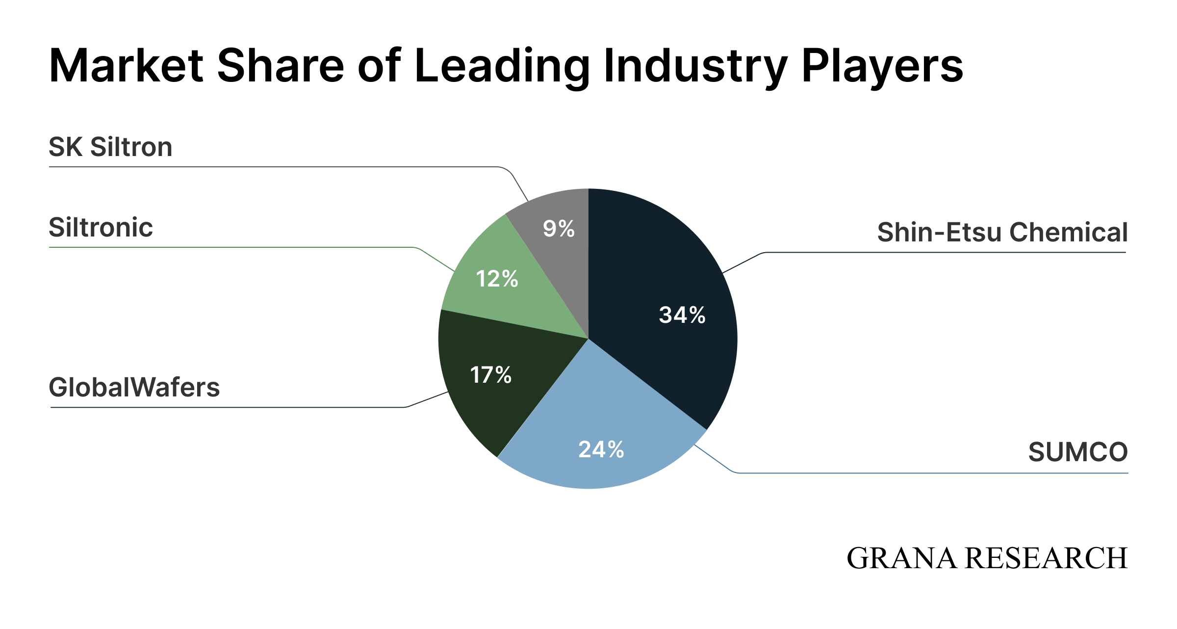
The silicon wafer market is a highly concentrated oligopoly dominated by companies with decades of accumulated process know-how. Five major players — Shin-Etsu Chemical, SUMCO, GlobalWafers, Siltronic, and SK Siltron — account for more than 90% of the market. Moreover, the two largest suppliers, Shin-Etsu Chemical and SUMCO, together control more than 50%.
In 2020-2022, amid a surge in end-market demand and supply-chain disruptions, semiconductor manufacturers rushed to secure wafer volumes years in advance. In response, wafer suppliers, backed by long-term agreements, shifted from incremental capacity upgrades to large-scale greenfield expansion. This dynamic ultimately led to an unprecedented inventory build-up that the industry has been working through until recently.
The rapid capacity expansion across the semiconductor industry is expected to drive substantial growth in silicon wafer demand. DRAM alone, including HBM, could generate incremental wafer demand of approximately 560,000 wafers per month by the end of 2027.
However, wafer manufacturers are reluctant to pursue further capacity expansion because the economics do not work at current ASPs. We expect the wafer market to enter a major pricing cycle. The previous 2017-2018 supercycle provides a useful reference point, when prices for 300 mm wafers increased by approximately 50% over two years.
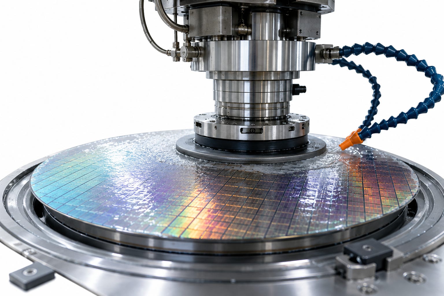
The Product Behind Every Chip
Every semiconductor chip begins its life not in an Nvidia R&D lab or at a TSMC fab, but at the bottom of a quarry — as a piece of quartzite. Cargo ships carry this quartzite to the Norwegian town of Holla, where it is smelted at 2,000°C to produce metallurgical-grade silicon. It is then transported to Wacker’s facility in Burghausen, where the silicon is converted into gas, passed through distillation columns, and deposited back into solid form, producing polysilicon with a purity of 99.9999999999%, or 11-12N. This corresponds to just one impurity atom for every trillion silicon atoms.
Wacker crushes the polysilicon rods under specialized cleanroom conditions into larger chunks (~30-100 mm) and smaller chips (~5-30 mm). The resulting dark-gray fragments, with their characteristic metallic sheen, are then packaged and shipped to customers. Ironically, one of the world’s most technologically sophisticated products begins with an unremarkable gray rock.
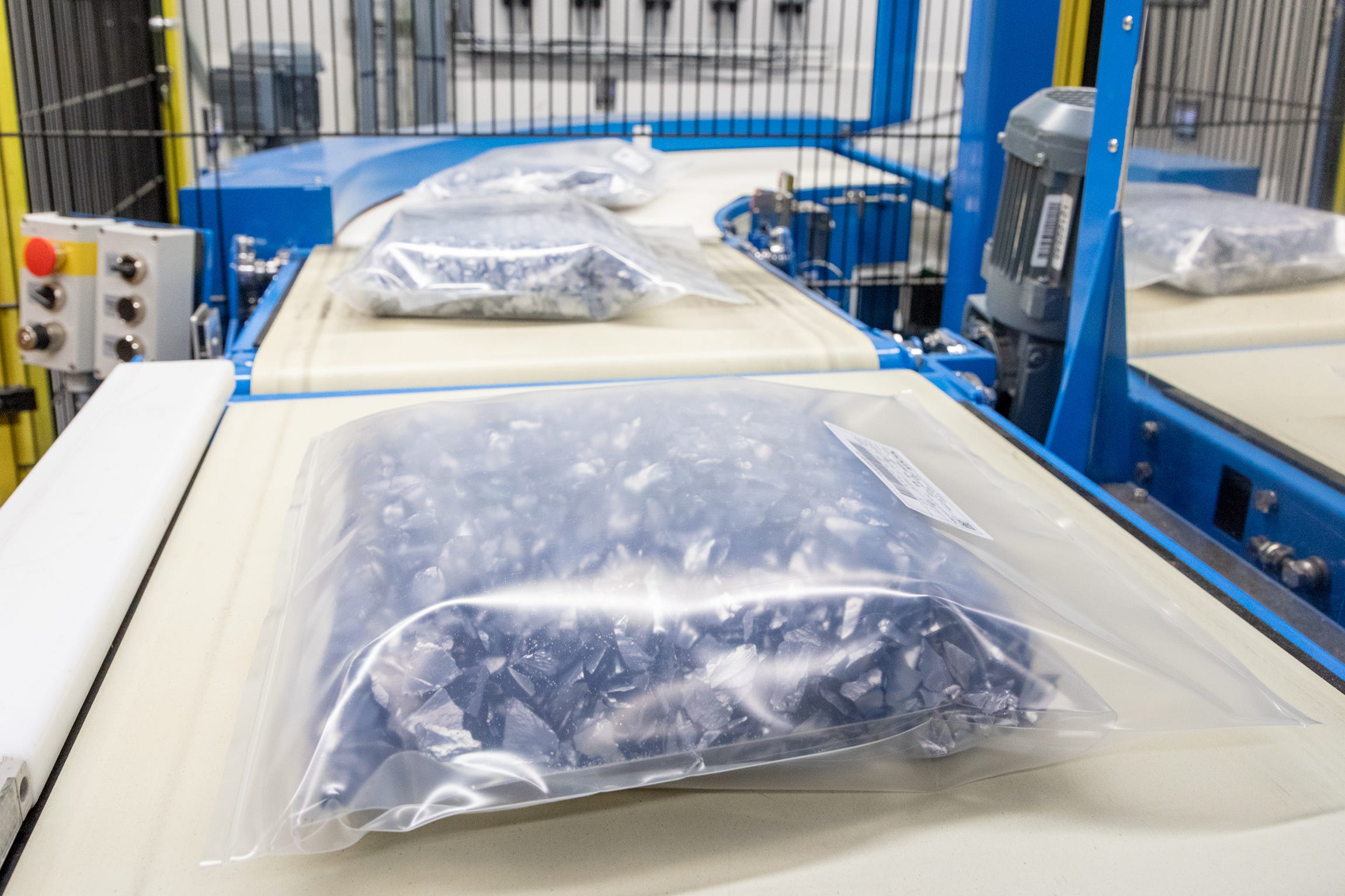
Semiconductor-grade polysilicon costs around $50-60 per kg ($23-27/lb), compared with approximately $5-7 per kg for solar-grade material. The price of 12N-purity polysilicon can be even higher, reaching $120-150 per kg [20].
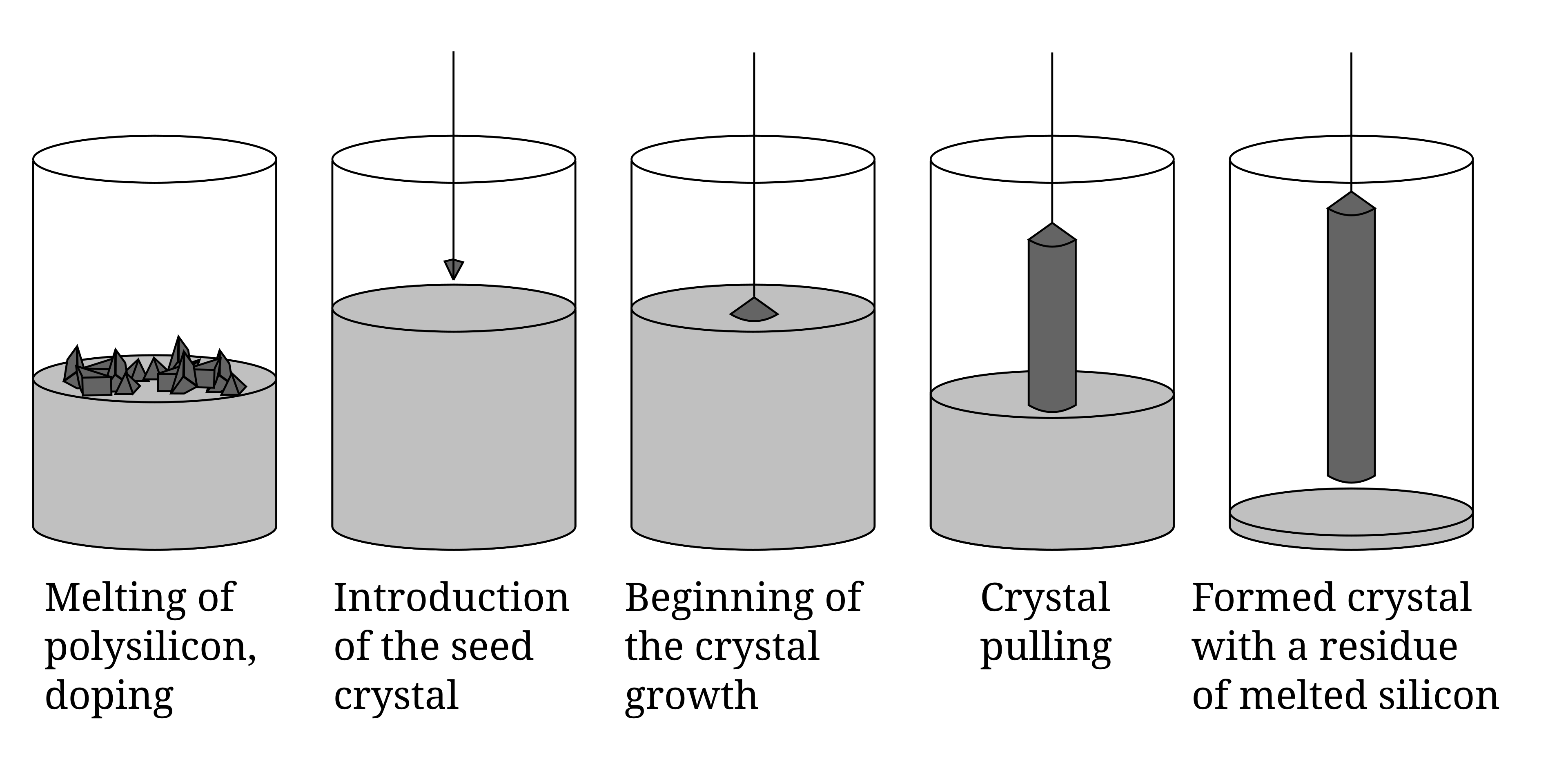
From this ultra-pure polysilicon, companies such as SUMCO, Shin-Etsu, and GlobalWafers produce silicon wafers. The process begins by loading 300-400 kg of polysilicon chunks and chips into a quartz crucible, where they are melted at approximately 1,420°C using a surrounding graphite heater heated by an electric current. A tiny seed crystal — a pencil-sized piece of silicon with the desired crystal structure — is then slowly lowered into the molten silicon. It is subsequently pulled upward just as slowly while being rotated.
As the seed is withdrawn, atoms from the molten silicon attach to its underside and solidify, replicating its crystal structure. Layer by layer, over the course of 24-48 hours, this process produces a cylindrical single-crystal silicon ingot approximately 100-300 mm in diameter and weighing around 200-300 kg. This process is known as the Czochralski method.
The ingot is then ground to the required diameter (200 or 300 mm) and sliced over the course of 8-12 hours using a diamond wire saw into hundreds of wafers approximately 775 μm thick — slightly less than one millimeter. The wafers are then ground, chemically etched to remove the damaged surface layer, and subjected to chemical-mechanical polishing (CMP), which makes the surface almost perfectly smooth. The result is a mirror-like finish with an average surface roughness of less than 0.1 nanometers. For comparison, if a wafer were scaled up to the size of a football field, the largest bump on its surface would be less than 0.5 mm high. Such demanding standards are necessary because transistors only a few nanometers in size will ultimately be fabricated on the wafer.
Each finished wafer is inspected across more than 50 parameters — including geometry, flatness, crystal lattice defects, and surface cleanliness — before being sealed in an airtight container under cleanroom conditions and shipped to customers such as TSMC, Samsung, or Intel.
The full manufacturing process, from crystal growth to the packaging of finished wafers, is well illustrated in this video:
Silicon wafers are classified according to several key characteristics, including diameter, crystal structure, surface treatment, and specialized applications for specific technologies, such as AI or power electronics. The primary classification is based on wafer size and processing technology:
Size (primarily 200 mm and 300 mm diameter)
Processing type (polished wafers vs epitaxial wafers)
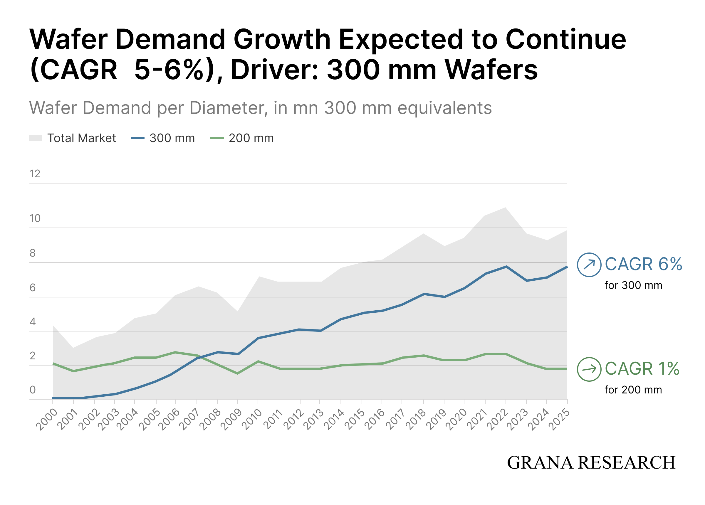
Newer, more advanced 300 mm wafers have 2.25x the surface area of a 200 mm wafer but cost only 1.3-1.5x as much to process. This translates into a 30-40% reduction in cost per die when migrating from 200 mm to 300 mm. The 200 mm format served as the industry workhorse throughout the 1990s and 2000s and today primarily supports older-generation manufacturing, including automotive MCUs, industrial sensors, power management ICs, and RF components.
Fabs built in the 1990s and 2000s continue to use 200 mm wafers because their equipment was designed around this wafer size, while the cost of retooling an entire fab would exceed the potential savings per die. However, as older capacity is gradually retired, the transition toward 300 mm wafers will continue.
The transition has been rapid. Major semiconductor manufacturers such as Texas Instruments aim to increase the share of their internal production running on 300 mm wafers to 80% by 2030, inevitably reducing their demand for 200 mm substrates [5]. Today, on a surface-area basis, 200 mm wafers account for approximately 20% of the total market.
After the crystal is sliced and polished, there are two main product categories: polished wafers (PW) and epitaxial wafers (epi). A polished wafer is essentially the finished slice of a silicon crystal, polished to extreme smoothness through the CMP process described above. It is a more commoditized product and is therefore more exposed to industry cycles. The memory market (DRAM and NAND) is the largest consumer of PW wafers, while a significant share is also used to manufacture simpler controllers and chips on legacy nodes, as well as for monitoring and test wafers used to calibrate semiconductor equipment. Approximately 75% of all 300 mm wafers are polished wafers.
Because a large share of wafer shipments is made under long-term contracts with terms of three to five years, available pricing data varies considerably. For example, a former ON Semiconductor manager estimated the price of a 300 mm wafer at $125-130 in 2023 [20]. However, based on our calculations using SUMCO data, the ASP for these wafers appears to be closer to $90-100.
The product mix also matters significantly. Wafers with the lowest defect levels are sold as high-grade products to customers such as Intel, TSMC, and Samsung for 5 nm processes, commanding the highest prices. Wafers that do not meet this threshold can instead be used for 14 nm or 28 nm nodes, with pricing differentiated by grade.
An epi wafer starts with the same polished wafer, which serves as the substrate (or handle wafer). A thin layer of single-crystal silicon — the epitaxial layer — is then grown on the PW surface in a specialized reactor. This additional layer has a more perfect crystal structure than the underlying wafer, resulting in fewer defects, better electrical properties, and higher manufacturing yields for the chipmaker. The epi layer enables the wafer to meet the extremely demanding specifications required for leading-edge logic at 3 nm and 2 nm.
Epitaxial wafers are typically manufactured to customer-specific specifications. Each fab operates a unique manufacturing process with its own equipment parameters, lithography requirements, and thermal conditions, meaning that the wafer must be tailored to that specific process. In other words, a supplier does not simply sell a “300 mm epi wafer” — it sells a “300 mm epi wafer built to TSMC N3 specifications,” which differs from one designed to “Samsung 3GAE specifications.” This customization allows wafer manufacturers to achieve higher margins and more stable pricing compared with polished wafers.
“That said, as I have been saying at each of our recent meetings, 300-millimeter epitaxial wafers are used in made-to-order products while 300-millimeter polished wafers are used for memory, which is typically produced in anticipation of demand and, therefore, has a tendency to overshoot. So it is necessary to take into consideration not only wafer inventory levels but end product inventory levels as well, which appear to be high. As such, a recovery in polished wafers is likely to take more time than epi in my view.” — Mayuki Hashimoto, CEO & Chairman at Sumco [7].
As with polished wafers, there is no publicly available data on the average pricing of epitaxial wafers. Based on our estimates, their ASP is approximately $130-140, depending on the complexity of the product and contract terms. For the most advanced solutions, prices can reach $240-250 per wafer, for example, for wafers used in CMOS image sensors.
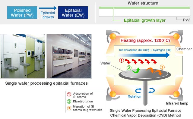
Thus, epitaxial wafers are significantly more expensive than polished wafers and require more sophisticated manufacturing equipment and deeper process know-how.
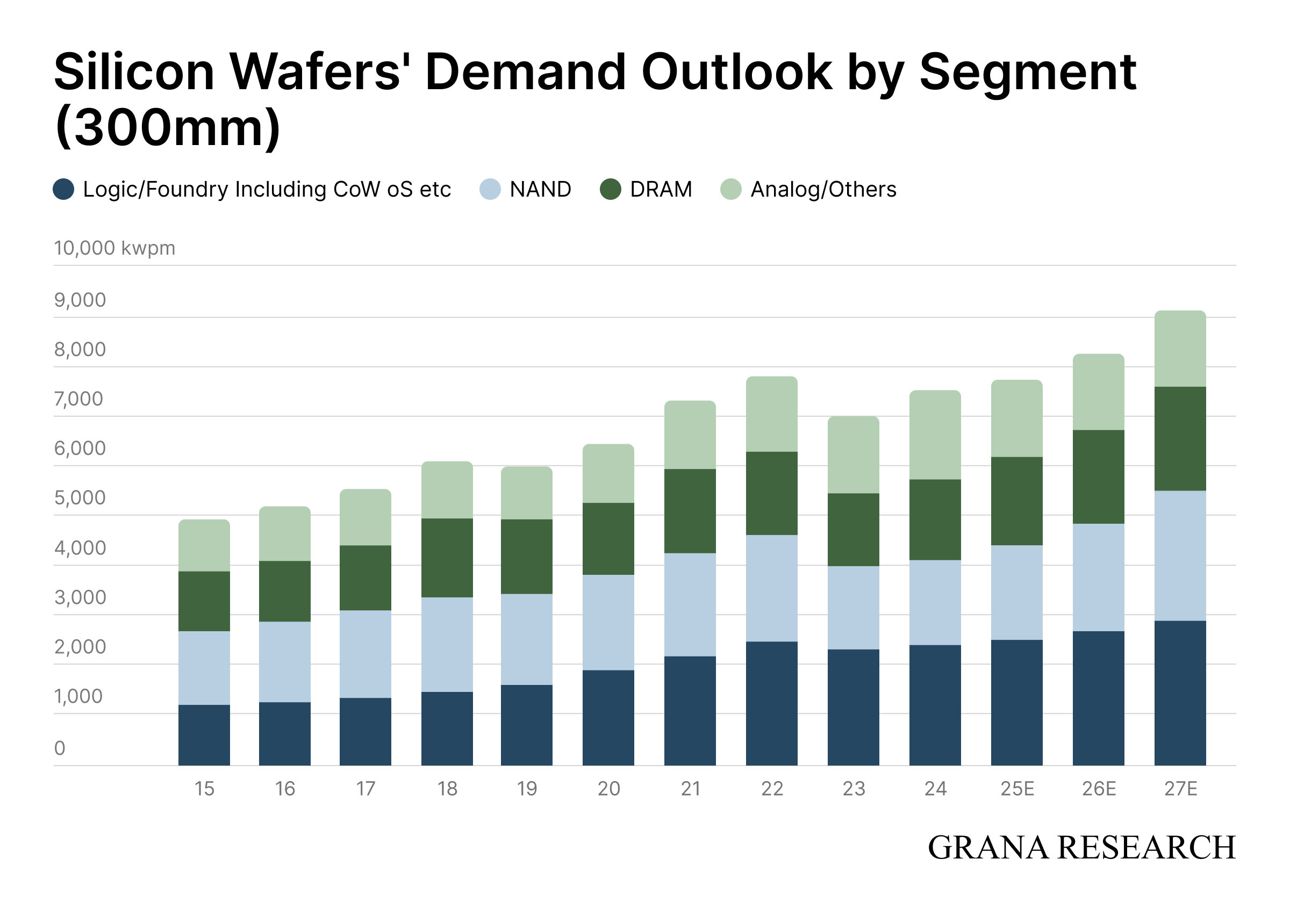
These extreme technical requirements help explain why the industry is a highly concentrated oligopoly dominated by companies with decades of accumulated process expertise. There are five major players in the market: Shin-Etsu Chemical, SUMCO, GlobalWafers, Siltronic, and SK Siltron. Together, they account for more than 90% of the market. Moreover, the two largest players — Shin-Etsu Chemical and SUMCO — alone control more than 50%.
Decades of process refinement and collaborative development with TSMC, Samsung, and SK Hynix create barriers that capital alone cannot replicate. You can build a wafer fab in three years, but you cannot replicate decades of accumulated process know-how in three years.
When a memory maker qualifies a new wafer supplier for HBM production, it must run thousands of test wafers through the full process flow, measure yields, correlate defect patterns, optimize process parameters, and validate reliability. This process takes 12-24 months and consumes engineering resources that could otherwise be devoted to production optimization. Even if the new supplier’s wafers perform well in testing, the customer faces switching costs in the form of lost engineering productivity and the risk that those yields may not translate to production scale. The rational decision is almost always to stay with the incumbent.
The economics further reinforce the moat. A silicon wafer accounts for roughly 3-5% of the total cost of the finished semiconductor device. But a defective wafer that causes yield losses can destroy value worth 10-50x the wafer’s price. This asymmetry means that, for advanced applications, customers are willing to pay a significant premium for wafers with proven, consistent quality rather than risk significant yield losses to save a few dollars per wafer. The value-to-cost ratio is so skewed that price sensitivity effectively disappears at the leading edge.
The table below outlines the approximate revenue mix for each of the “Big Five” in the wafer segment. These figures are derived from official company disclosures, earnings presentations, and Tegus expert interviews.
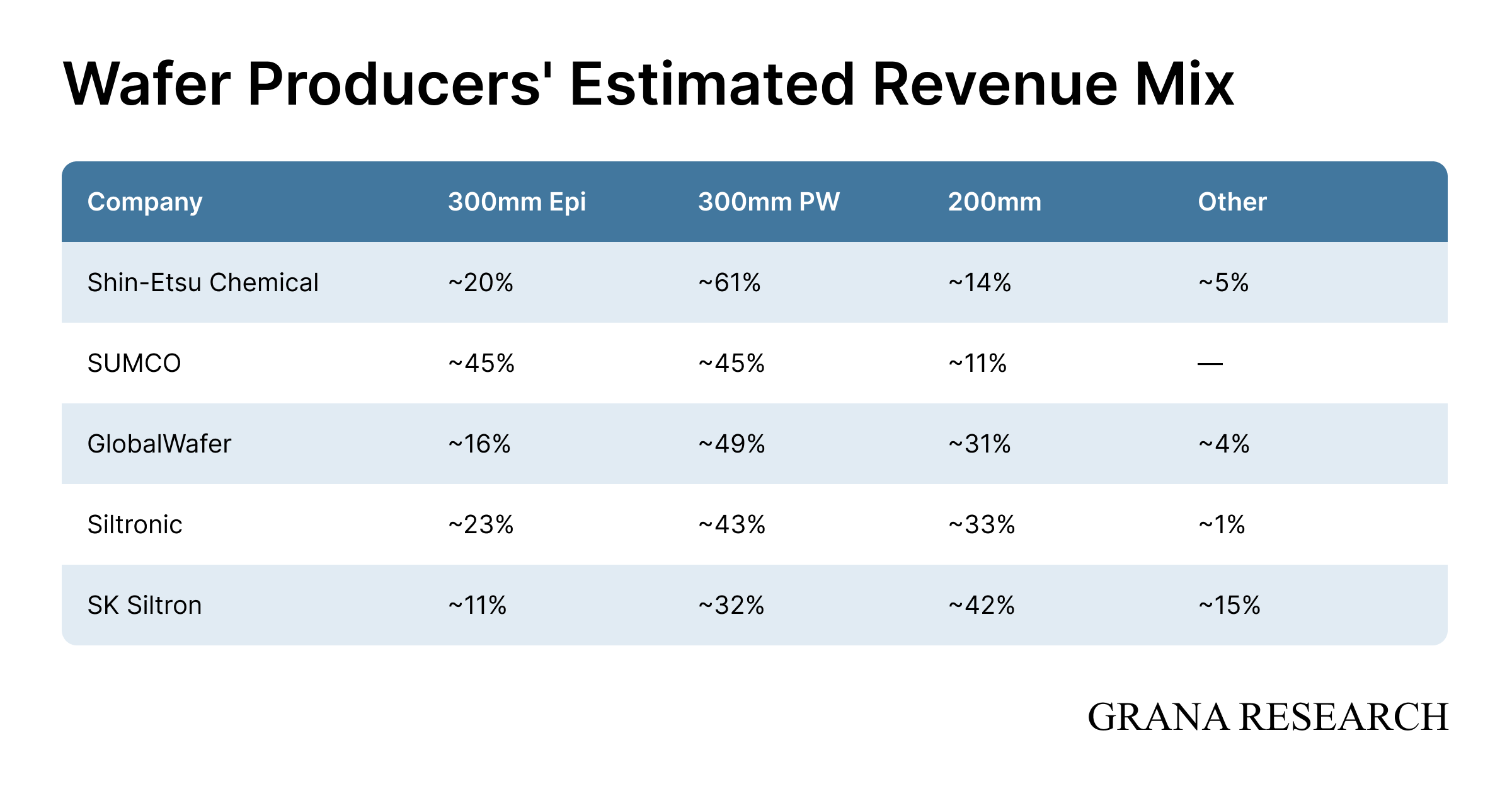
Shin-Etsu and SUMCO have the highest concentration in advanced 300 mm epitaxial wafers, precisely where AI demand is strongest, and margins are highest. GlobalWafers’ 200 mm exposure (35-43% of revenue) is the largest among the majors, limiting its AI upside but providing optionality if the 200 mm market stabilizes. SK Siltron data is estimated from limited public disclosure; the company is privately held within the SK Group and does not report a granular product mix.
Anatomy of a Wafer Cycle
The stability of these market positions is reinforced by how the industry structures its commercial relationships and capacity investments. The silicon wafer industry has a structural feature that creates a real investment opportunity: massive time lags between capex decisions and capacity coming online. Building a new wafer fab takes approximately three years from groundbreaking to production. These long lead times apply equally on the demand side: Micron’s new Idaho chip fab, for example, is on a three-year construction schedule, with production expected by 2027. Each new chip fab of this scale represents incremental wafer demand that is locked in years before the first lot runs. This matters for two reasons: when demand surges, supply cannot respond quickly; and when investment decisions made during booms bring capacity online just as demand softens, the result is an extended period of oversupply.
Customer relationships in the industry are governed by long-term agreements (LTAs). The process begins with a foundry receiving an 18-36-month forecast of end demand from its customers. The foundry then passes this demand signal upstream to wafer suppliers, providing roughly six months of additional forward visibility — a total horizon of 24-42 months — beyond the duration of its own customer contracts. The parties then enter into LTAs, typically with terms of three to five years.
During periods of strong demand and heavy investment in new production capacity, companies may enter into agreements lasting five to six years. In such cases, capacity expansion projects are often tied to customer commitments to purchase output for up to five years after the new capacity comes online.
These contracts typically include commitments to purchase specified volumes and tightly define product specifications, including substrate type, diameter, crystal quality, flatness, and defect density. Most contracts are based on fixed pricing, although some incorporate step-up mechanisms under which prices increase annually, for example, by 2-3%. Customers generally cannot cancel these contracts.
However, this mechanism — designed to protect wafer manufacturers from the industry’s inherent cyclicality — ultimately became the source of the unprecedented headwinds they have faced in recent years.
During the pandemic in 2020-2022, a sharp surge in end-market demand and widespread supply-chain disruptions pushed semiconductor manufacturers and their customers to secure access to critical components at almost any cost. As a result, major foundries and IDMs aggressively entered into LTAs with silicon wafer suppliers, locking in volumes several years in advance. Against this backdrop, wafer manufacturers shifted from incremental upgrades to existing production lines toward large-scale construction of new fabs. Importantly, much of this planned capacity had already been committed to customers under LTAs before construction even began.
The following excerpt from GlobalWafers’ Q4 2021 earnings call is particularly illustrative:
“At end of — as of end of 2021, the amount of our prepayment balance reached TWD 28.6 billion or around USD 1 billion. And this is TWD 6.2 billion higher than our prepayment balance as of the end of Q3. So in Q4 only, this one quarter, we received another new TWD 6.2 billion new prepayment — TWD 6.2 billion prepayment or USD 0.2 billion. And this prepayment amount keeps increasing in 2022 as well.
Our capacity expansion as we announced to the market that we have our brownfield and greenfield big capacity expansion. Overall, global digital transformation accelerated by COVID-19 has propelled the demand for cloud services -- server and also high-performance computing. 5G is rolling out an unprecedented pace and its uptake is far faster than 4G, so embodying people’s need for connectivity. Yes, connectivity, this is the key word for the growth. And those technological advancements and increasing silicon content could not be achieved under current level of worldwide semiconductor production capacity. Therefore, we are seeing very aggressive expansion program announced by almost all the key 1 — the key Tier 1 players, all key players in all sectors of semiconductor supply chain” — Hisu-Lan Hsu, Chairperson & CEO
In September 2021, SUMCO decided to invest a total of ¥228.7 billion ($2.08 billion) to expand its 300 mm epitaxial wafer production capacity. The company’s capital expenditures increased from ¥69.5 billion ($0.63 billion) in FY2021 to ¥130.8 billion ($1.05 billion) in FY2022.
Market leader Shin-Etsu pursued a more gradual expansion strategy, focusing on meeting demand through brownfield projects. Capital expenditures in its Electronic Materials segment totaled ¥106.5 billion ($0.97 billion) in FY2021, while the company guided to ¥300 billion ($2.40 billion) in FY2022 capex for the group as a whole.
Taiwan-based GlobalWafers redirected funds originally earmarked for the acquisition of Siltronic toward aggressive organic capacity expansion. In early 2022, the company announced a three-year capital expenditure plan (2022-2024) totaling TWD 100 billion ($3.57 billion). Approximately 55% of this amount was allocated to greenfield projects, including a new fab in Texas, while the remaining 45% was earmarked for expansions at existing facilities across six countries.
Germany-based Siltronic embarked on the largest investment project in its history. The company’s capital expenditures more than doubled, from €425.6 million ($0.46 billion) in 2021 to €1,073.6 million ($1.16 billion) in 2022.
The financial footprint was unprecedented. Sector capex roughly tripled — from a steady-state run rate of $1.5-1.8 billion per year in 2018–2021 to $3.8 billion in 2022 — before peaking at approximately $5.5 billion in 2023, followed by another $4.8 billion in 2024. Cumulative spending over 2022-2024 reached roughly $14 billion.
According to SUMCO estimates, global 300 mm wafer production capacity increased from approximately 6.0 million wafers per month in 2020 to more than 8.0 million wafers per month in 2022.
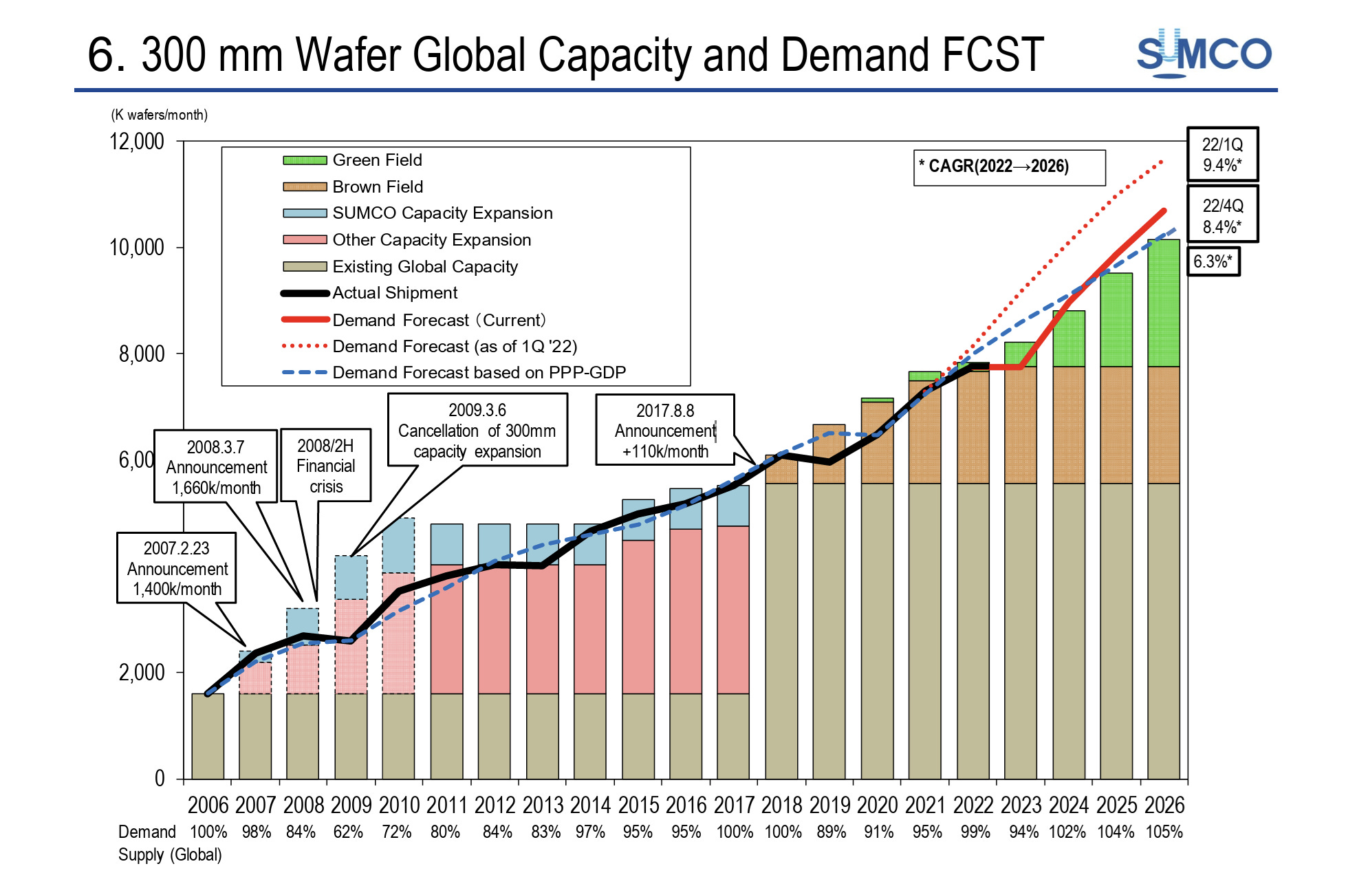
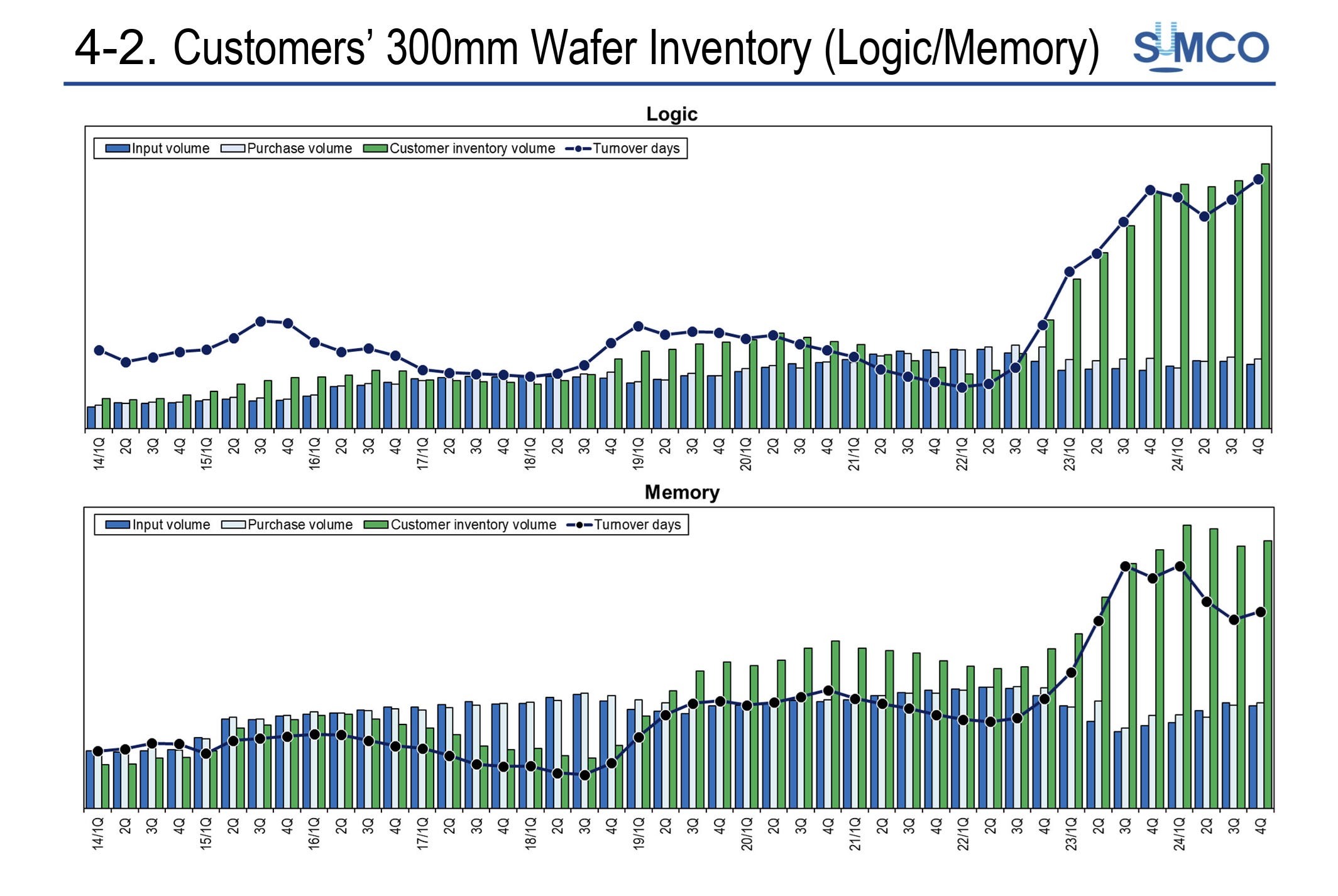
However, headwinds began to emerge as early as Q4 2022: shipments started to decline, while customer inventories rose rapidly, particularly in logic. Nevertheless, the prevailing industry view remained that LTAs and prepayments would cushion the cycle, as they had in 2019. The first warning sign came from Siltronic. In early February 2023, the company released preliminary results for 2022, providing a cautious but broadly neutral-to-optimistic outlook. Just one month later, Siltronic published its final results, highlighting a sharp deterioration in market conditions and order push-outs from customers.
The second, even stronger signal came from GlobalWafers. The company disclosed that, under the terms of its contracts, it had returned a portion of customer prepayments because customers had failed to take the volumes they had originally committed to purchase.
The third and clearest signal came from SUMCO. In February 2023, the company projected 2024 demand at 102% of supply — a tight, undersupplied market. By November 2023, that figure had been cut to 76%. The industry went from “structurally short” to “structurally long” in a matter of months.
On the one hand, LTAs supported revenues and pricing, as customers largely continued to honor their contractual commitments. On the other hand, those same LTAs forced customers to continue taking wafers they no longer needed, contributing to a further build-up of inventories.
Wafer manufacturers did not respond with panic. Even amid weak market conditions, SUMCO noted that customers continued to honor LTA pricing, while the company was still able to implement previously agreed price increases. In other words, the adjustment did not come through price capitulation, but rather through active management of shipment volumes and delivery schedules.
Manufacturers began accommodating push-outs, delivery adjustments, and delays. By early 2024, SUMCO management explicitly stated that, given extremely high customer inventories, the company had “no choice but to cooperate with customer requests to delay deliveries.”
At the same time, manufacturers began cutting production and slowing the ramp-up of new capacity. SUMCO, for example, continued with its domestic expansion projects but slowed the capacity ramp at its Taiwan/FST operations, which had greater exposure to polished wafers, where the correction was more severe.
Around the same time, a new structural challenge for the industry began to emerge: the accelerating entry of Chinese producers into the market. Chinese wafer manufacturers have made impressive progress, with combined capacity estimated at 1-2 million wafers per month across 200 mm and 300 mm wafers. According to J.P. Morgan, the market share of Chinese companies increased from 2.7% in 2021 to 19.4% in 2024 and is on track to exceed 30% [19]. However, it is important to note that Chinese producers are particularly strong in the 200 mm market, which primarily serves mature nodes.
By 2024, the industry recovery had become increasingly selective. The 300 mm segment, particularly applications related to AI and leading-edge technologies, was recovering more strongly, while 200 mm and smaller-diameter wafers remained weak. Shin-Etsu highlighted this divergence in demand particularly clearly. During an earnings call, management emphasized that, in the current market environment, only AI-related semiconductor devices were performing well, while other end markets remained stagnant.
Siltronic took the most decisive action: in March 2024, the company announced that it would exit the small-diameter wafer business by 2025, explaining that the segment had become too small and was facing intensifying competitive pressure from Chinese suppliers.
By May 2024, SUMCO’s CEO confirmed that 300 mm wafers had passed the bottom of the cycle, while 200 mm wafers continued to “crawl along the bottom.” Nevertheless, even in the 300 mm segment, a meaningful recovery in wafer consumption at semiconductor fabs did not translate into higher wafer purchases, as customers prioritized drawing down their existing inventories.
Overall, 2024 and 2025 remained years of sharp polarization, with explosive demand for AI-related products contrasting with prolonged stagnation across consumer and industrial end markets. At the same time, the industry faced an unprecedented increase in depreciation expenses as major investment programs reached completion, putting significant pressure on profitability in 2025 and contributing to a cautious outlook for 2026.
It was not until November 2025 that the shipment trend finally returned to 2022 levels, the industry’s previous peak. For the full year, global silicon wafer revenue reached $11.4 billion, with total shipments of 12.97 billion square inches (MSI). Shipments of 300 mm wafers averaged approximately 7.7 million wafers per month against installed capacity of roughly 8.8 million wafers per month, implying approximately 13% excess capacity in the 300 mm segment — or roughly 87% utilization. This supply-demand imbalance lies at the heart of the current cycle.
From Oversupply to Shortage
The inflection point for the industry came in late 2025 and early 2026, when the rapid increase in prices for memory and other AI infrastructure components triggered a sharp upward revision in industry capex expectations. In early March, GlobalWafers Chairwoman and CEO Doris Hsu told institutional investors that prices for both 200 mm and 300 mm wafers had bottomed in Q4 2025 — Q1 2026, rush orders were beginning to emerge, and advanced 300 mm capacity was fully utilized. By August, following the company’s latest reporting period, management noted that capacity was fully utilized across all segments and that supply of certain advanced 300 mm wafers had already become noticeably tight [19].
Executives at other companies also became significantly more optimistic about supply-demand dynamics. In May, SUMCO management noted that the company was still in recovery mode: customer inventories were declining, while some equipment remained underutilized. By August, however, President Ryuta highlighted that capacity utilization was approaching 100%, customers were increasingly concerned about securing sufficient wafer volumes for 2027-2028, and some were already considering rebuilding inventories. According to SUMCO, the 300 mm wafer market grew by approximately 15% year over year in Q1 2026 [19].
While expectations remained cautious at the beginning of the year, concerns about a potential shortage of leading-edge wafers have since intensified, prompting major customers to secure future supply. Micron Technology, for example, announced a strategic partnership with GlobalWafers involving a $500 million investment to expand U.S. silicon wafer production capacity, alongside a 10-year supply agreement that guarantees Micron access to significant volumes of 300 mm wafers. SK Group also abandoned its earlier plans to sell wafer manufacturer SK Siltron to Doosan [19].
Several factors are driving wafer demand and contributing to the expected supply shortage, including the memory supercycle, growth in leading-edge logic, and a recovery in mature nodes.
If you are even remotely familiar with the stock market, it is no secret that the memory industry is experiencing one of the most impressive upcycles in its history. While the prevailing view last year was that price increases would normalize within a reasonable timeframe, the consensus today is increasingly that the supply-demand imbalance is here to stay. Against the backdrop of LTAs signed with their customers — an interesting parallel with the wafer market — leading memory manufacturers such as Samsung, SK Hynix, and Micron have begun radically revising their investment and capacity expansion plans.
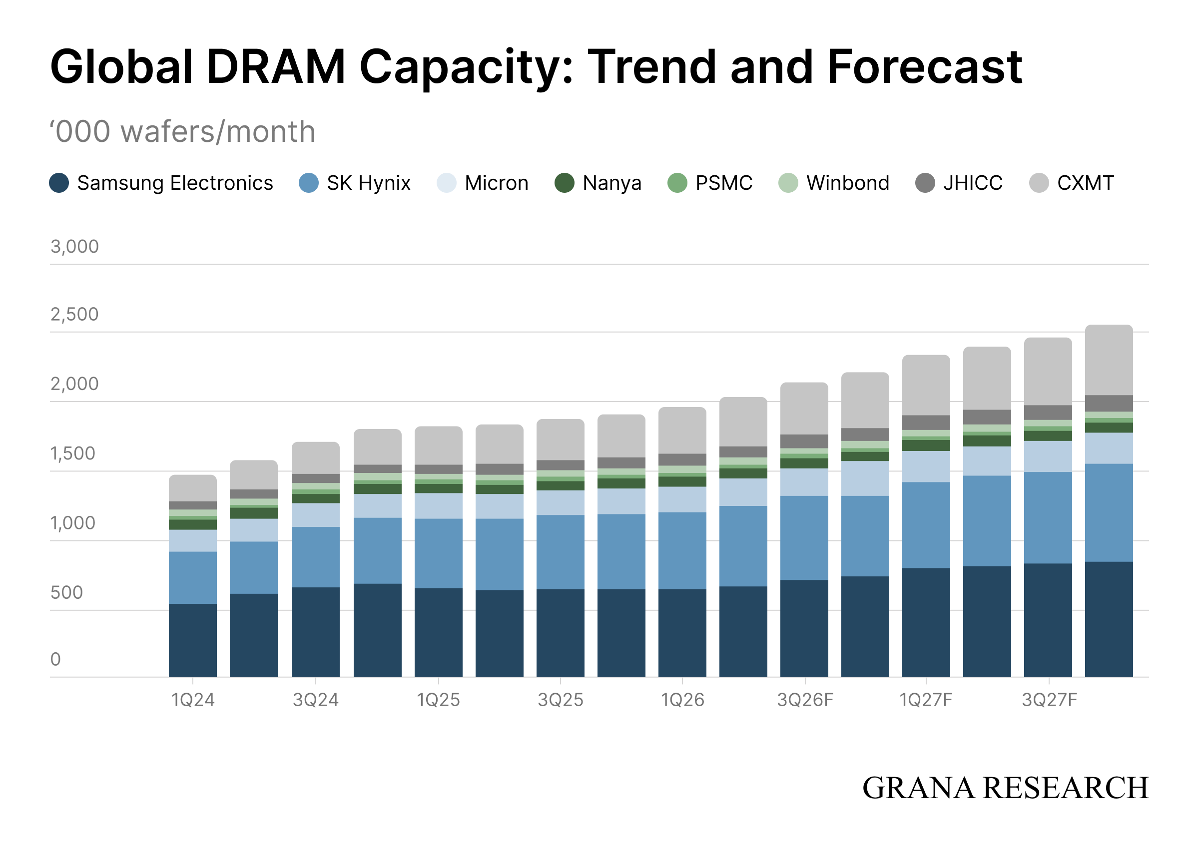
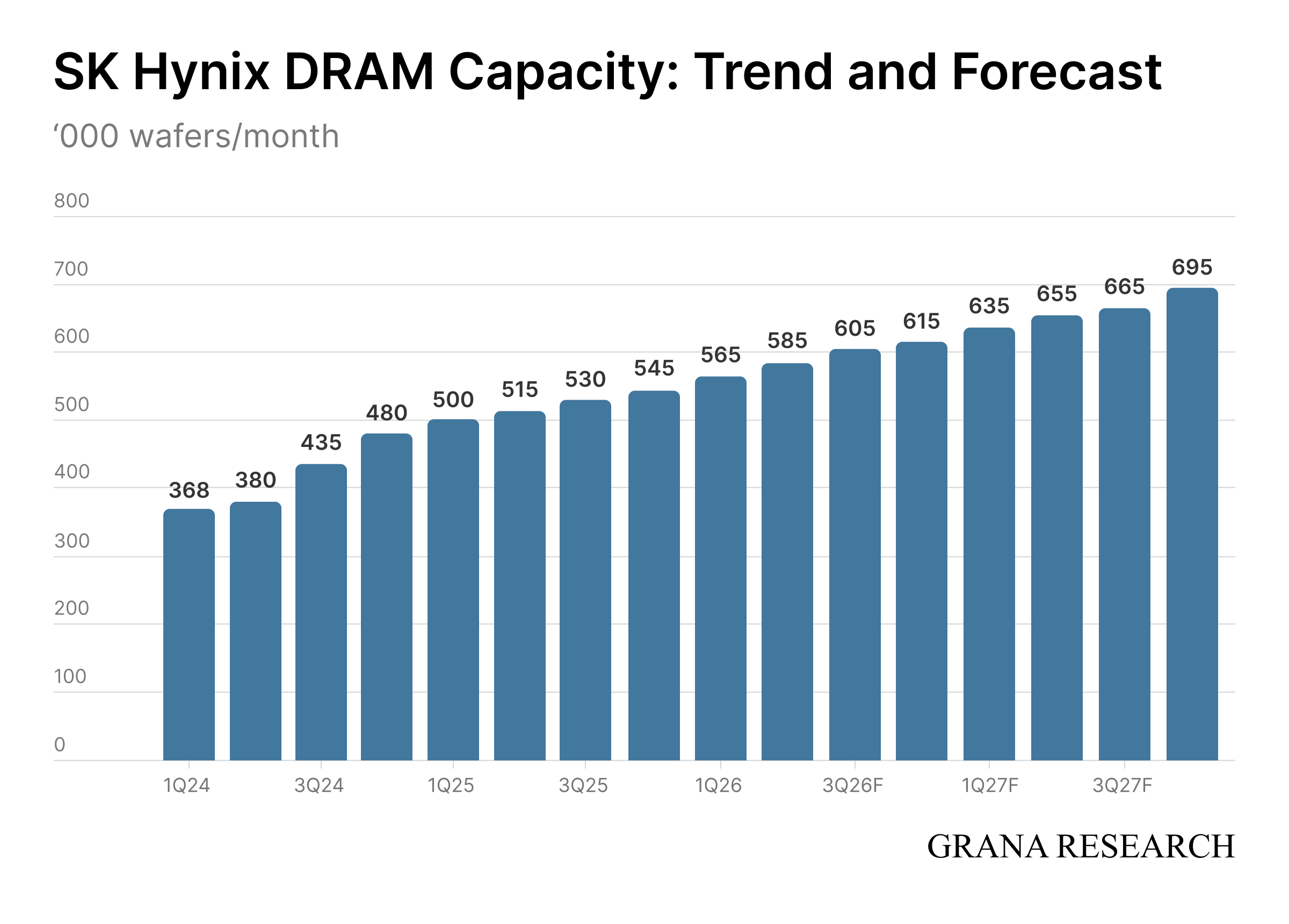
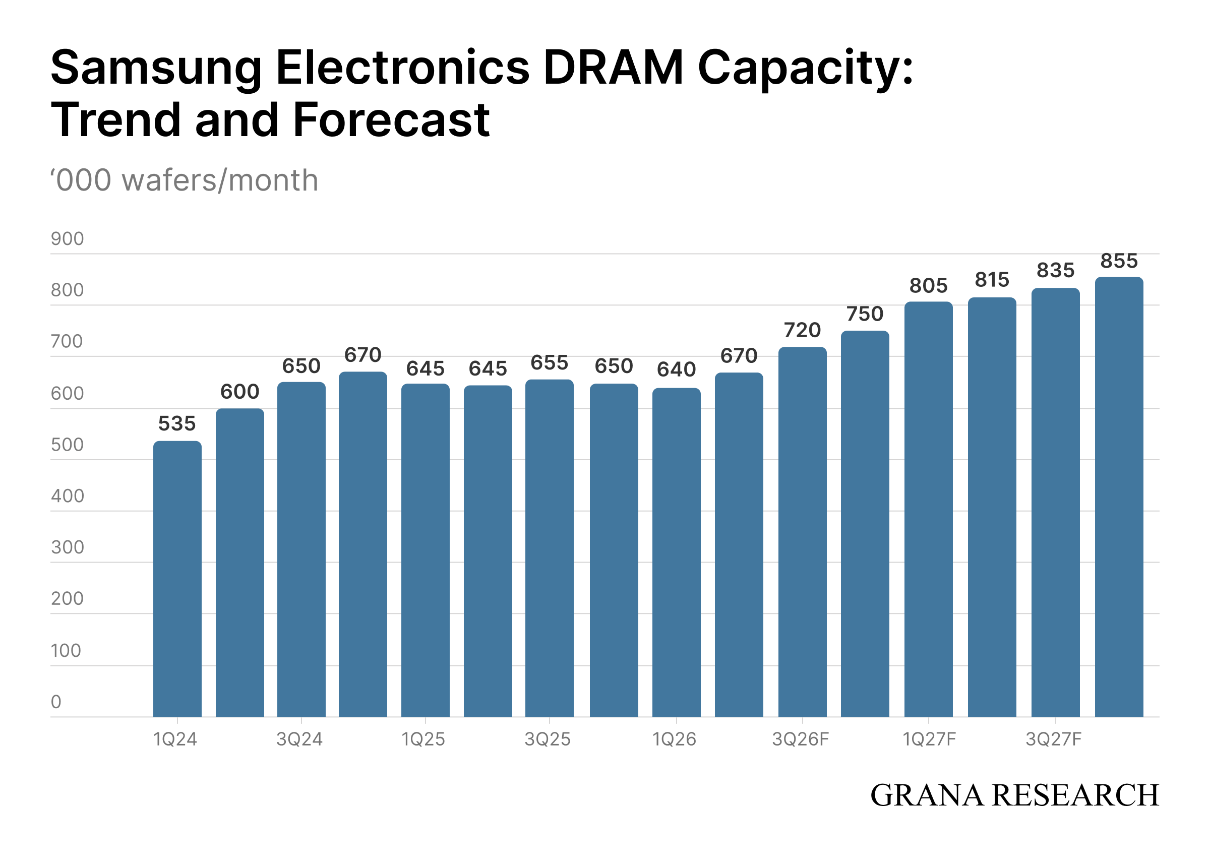
Samsung Electronics plans to increase its DRAM capacity from 640,000 wafers per month in Q1 2026 to 855,000 wafers per month by Q3 2027. SK Hynix is expected to expand its DRAM capacity from 565,000 wafers per month in Q1 2026 to 695,000 wafers per month by Q3 2027. According to TrendForce estimates, global 300 mm DRAM wafer capacity is expected to increase from 1.64 million wafers per month in 2024 to more than 2.5 million by the end of 2027. Over the longer term, total DRAM capacity is expected to increase by 2-3x compared with 2024 levels. Samsung Electronics’ capacity, in particular, could reach 1.35 million wafers per month, while SK Hynix could reach 1.0 million wafers per month by 2030 [19].
Equally important, HBM is accounting for a growing share of the production mix. According to Deutsche Bank estimates, HBM’s share of total DRAM bit production is expected to increase from approximately 5% in 2025 to around 10% by 2030. HBM production requires significantly more silicon wafers than conventional DRAM for the same amount of memory capacity. Specifically, HBM requires roughly three times more silicon wafer area per bit than conventional DRAM, while for HBM4/HBM4E, the ratio could reach 4:1 [20].
As a result, DRAM alone, including HBM, could generate incremental silicon wafer demand of approximately 560,000 wafers per month by the end of 2027. If the capacity expansion plans outlined by Samsung Electronics and SK Hynix are fully implemented, incremental wafer demand from these two manufacturers alone could exceed 1.1 million wafers per month by 2030.
Similar trends are emerging in leading-edge logic. To address the capacity shortage for AI chips, TSMC raised its 2026 capex guidance to $60-64 billion. The company expects investment over the next three years to be significantly higher than over the previous three. Based on our estimates, TSMC alone could generate incremental wafer demand of approximately 280,000-320,000 wafers per month by 2028.
A second tier of capacity additions could contribute another 100,000-120,000 wafers per month over the same horizon. Intel has reached approximately 30,000 wafers per month on its 18A process after addressing yield issues, with Fabs 52 and 62 designed for combined capacity of up to 40,000 wafers per month [14]. Samsung Foundry is targeting 50,000 wafers per month of SF2/SF3P capacity in Taylor, with a mature ramp realistically achievable by 2028 [15]. Rapidus, meanwhile, is expected to launch a pilot line with capacity of approximately 10,000 wafers per month from 2027 [16]. Combined, these additions imply incremental capacity of approximately 380,000–440,000 wafers per month.
SEMI expects advanced-node capacity (≤7 nm) to increase from 850,000 wafers per month in 2024 to approximately 1.4 million wafers per month by 2028, representing a CAGR of roughly 14% and implying approximately 550,000 wafers per month of incremental demand from leading-edge logic alone [15].
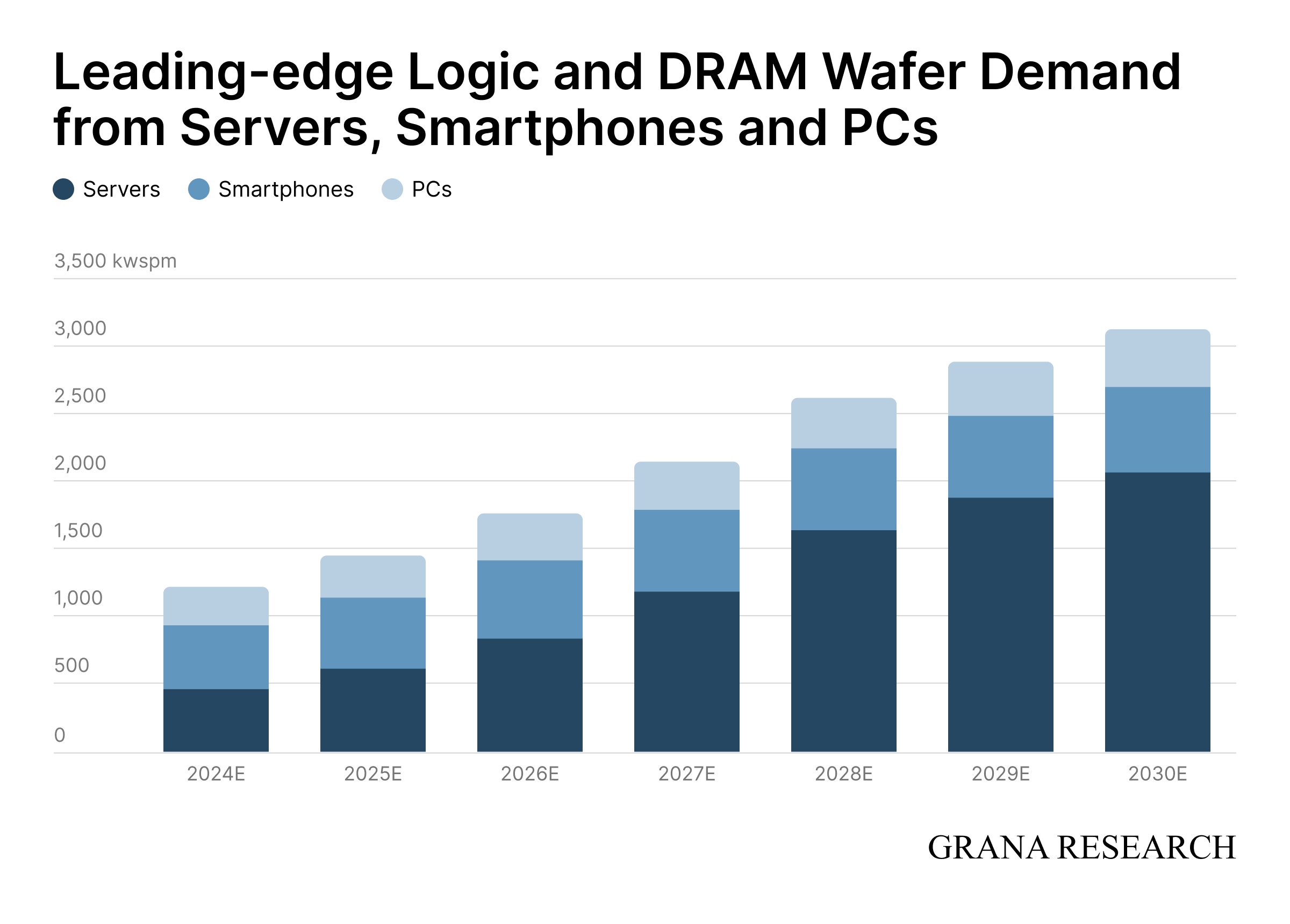
Thus, the current fab investment cycle is set to generate substantial incremental demand for silicon wafers. According to Barclays’ estimates, combined demand for leading-edge logic and DRAM wafers used in servers, smartphones, and PCs is expected to grow at a CAGR of approximately 17% from 2025 through 2030, adding roughly 1.0 million wafers per month of demand between 2025 and 2028, followed by another approximately 0.5 million wafers per month between 2028 and 2030 [16].
According to CTEE, growing demand from AI servers and advanced chip manufacturing could push the global silicon wafer supply shortfall to 8% by the end of this year, 15% by the end of next year, and 24% by the end of 2028 [18].
Leading wafer manufacturers such as Shin-Etsu, SUMCO, and GlobalWafers have noted that their 300 mm wafer production lines are already operating at or near full capacity, while supply is becoming increasingly constrained.
“With regard to production for 300-millimeter, we are very close to full capacity utilization... We will truly be at full capacity utilization in Q4.” — SUMCO Q2 FY2026 conference call
Based on the experience of previous cycles, one might expect the next step to be another investment supercycle in the silicon wafer industry. However, comments from wafer manufacturers point to a different scenario: rather than aggressively expanding capacity, the market could move into a pronounced supply shortage, creating a seller’s market and setting the stage for substantial price increases.
A particularly noteworthy exchange took place between a Goldman Sachs analyst and SUMCO’s President during the company’s latest earnings call. The analyst noted that, based on their calculations, wafer prices would need to be roughly twice their current levels for capacity expansion to generate an adequate return. Management confirmed that a 5-10% increase in ASPs would clearly not be sufficient:
“GS’ Analyst:
I am Ikeda of Goldman Sachs. In looking at the silicon wafer projections for servers you have outlined for 2027 and 2028 on page 15, the numbers appear very conservative if you take into account the expected increase in chips per end product or CBA. Have you baked in some supply risk into your forecast?
For 300-millimeter, I expect 2027 to be very tight and expect to see shortages in 2028. Despite this backdrop, I understand that you are hesitant to commit to greenfield investments, as you alluded to earlier. If you use a hurdle rate that is close to your weighted average cost of capital, you would need to see a doubling of wafer prices to enable new investments, or the economics would not work at all. It means that prices need to be significantly different from current levels.
With the profitability improving significantly at your customers and structural demand growing, what sort of negotiations are you currently conducting? Are there measures you can put into place, such as requiring upfront payments or extending the tenure of the LTAs, to ensure that you can sustain profit growth over the longer term? Please comment to the extent you can, including lesson learned in hindsight.
SUMCO’s Jiro Ryuta:
There are many things that I regret in hindsight in many different fields, which makes it difficult to talk about in short. It is true that the forecast for server-use silicon wafer demand takes into account the fact that the supply side is not in a position to increase supply at this time. Actual demand levels are higher, but at this stage, it is not possible to grow supply. Demand is likely to exceed supply for more than three years, in my view, because of such supply constraints.
In terms of the price level that we would need to increase supply capacity and invest to expand supply, we have made no specific statement at this stage. But what I can say is my personal sense is that prices would need to be dramatically higher. To your point, I think an increase of 5% or 10% would not have a meaningful impact. That’s my impression.”
Siltronic management also confirmed that, while spot prices have begun to increase selectively, they have yet to reach levels that would justify large-scale investment in further capacity expansion. As a result, the company is taking a selective approach, prioritizing contracts with more attractive terms rather than simply pursuing volume growth [17].
As the market leader, Shin-Etsu has noted that it is actively negotiating price adjustments even under existing contracts. The company is discussing LTA price revisions with customers in response to sharp increases in electricity, raw material, and logistics costs. In the memory segment, the company is receiving requests for LTAs extending through 2028 [18].
According to SunSirs Commodity Data Group, starting in May, leading manufacturers issued successive price increase notifications, raising prices for standard 12-inch wafers by 3-8% and high-end AI-specific wafers by nearly 20%, resulting in a cumulative annual increase of more than 15% [19].
Thus, the silicon wafer industry is set to benefit from substantial incremental demand, while manufacturers, having learned from the previous cycle, are publicly resisting aggressive capacity expansion because the economics simply do not work at current ASPs. The key factor is the asymmetry in pricing: the substrate accounts for only 3-5% of the cost of a processed wafer at the fab, meaning that even a doubling of wafer prices would translate into only a 3-5% increase in chip manufacturing costs — an amount that pales in comparison with the cost of leaving leading-edge capacity idle. The logical outcome is one of the most significant pricing cycles in the industry’s history, with the previous 2017-2018 supercycle providing a useful benchmark, when 300 mm wafer prices increased by approximately 50% over two years.
Sources
[1] https://www.wacker.com/cms/en-us/press-and-media/press/press-releases/2024/detail-228484.html
[2] https://en.wikipedia.org/wiki/Czochralski_method
[3] https://www.sumcosi.com/english/products/process/step_01.html
[4] YouTube
[5] https://investor.ti.com/static-files/fc9d9346-cf77-40db-902a-e9961e9c5736
[6]https://www.siltronic.com/fileadmin/investorrelations/2025/Q4/20260312_Siltronic_InvestorPresentation.pdf
[7] Sumco Corporation, 2023 Earnings Call, Feb 14, 2024
[8] https://www.sumcosi.com/english/products/process/step_03.html
[9] https://reports.valuates.com/market-reports/QYRE-Auto-21H9107/global-single-crystal-silicon-wafers-300mm
[10] GlobalWafers Co., Ltd., 2021 Earnings Call, Mar 15, 2022
[11] https://ssl4.eir-parts.net/doc/3436/ir_material_for_fiscal_ym18/130842/00.pdf
[12] https://ssl4.eir-parts.net/doc/3436/ir_material_for_fiscal_ym18/172131/00.pdf
[13] https://www.kad8.com/ai/intel-reports-18a-yield-breakthrough-30000-wafers-per-month-capacity-and-14a-roadmap/
[14] https://www.tomshardware.com/tech-industry/semiconductors/samsungs-taylor-texas-fab-could-herald-a-breakthrough-for-the-chipmaker-company-plans-2026-risk-production-new-production-flows-pellicles-for-euv-patterning-as-site-targets-50-000-wspm
[15] https://www.semi.org/en/semi-press-release/semi-forecasts-69-percent-growth-in-advanced-chipmaking-capacity-through-2028-due-to-ai
[16] Barclays, European Technology Hardware: From GW to WFE II
[17] https://www.siltronic.com/en/investors.html
[18] https://www.taiwannews.com.tw/news/6419954
[19] Bloomberg
[20] AlphaSense
Disclaimer / Disclosures
The information contained in this report is provided solely for informational and educational purposes and does not constitute investment advice, investment research under applicable securities regulations, an offer to sell, or a solicitation to buy any security or financial instrument.
The opinions expressed in this report reflect the author’s views as of the date of publication and are subject to change without notice. This report has been prepared without regard to the specific investment objectives, financial situation, or particular needs of any individual investor. Readers should conduct their own independent research and seek professional financial, legal, tax, or other advice before making any investment decision.
The analysis presented in this report is based on information believed to be reliable, including publicly available sources, company disclosures, industry publications, and discussions with market participants. While reasonable efforts have been made to ensure the accuracy of the information, no representation or warranty, express or implied, is made as to its accuracy, completeness, or reliability. Any estimates, assumptions, or forecasts represent the author’s judgment and are inherently subject to uncertainty.
This report contains forward-looking statements, including expectations regarding future financial performance, industry trends, market developments, and company prospects. Such statements involve known and unknown risks, uncertainties, and assumptions that may cause actual results to differ materially from those expressed or implied. No assurance can be given that any projections or forecasts will be realized.
The author may hold, establish, increase, reduce, or dispose of positions in any securities discussed in this report at any time without prior notice. Such positions may create potential conflicts of interest. Nothing in this report should be interpreted as a recommendation to buy, sell, or hold any security.
To the fullest extent permitted by applicable law, the author disclaims any liability for any direct or indirect loss arising from the use of, or reliance upon, the information contained in this report.
SK Group also abandoned its earlier plans to sell wafer manufacturer SK Siltron to Doosan
SK Group did in the meantime sell SK Siltron to Doosan (https://www.businesskorea.co.kr/news/articleView.html?idxno=274026)
Well done solid write-up. Ozeco and I wrote about this about a week ago, similar conclusions. Something that's sticks with me that's it's not a commodity business as most would be led to believe. Wafers need to be customised on the surface to what the client needs. Thus the moat of the big 5 oligopoly is stronger than a pure commodity business.