


Summary
RS Technologies (3445 JP) evolved from a distressed asset — the 300mm wafer reclaim line that Rasa Industries sold for a fraction of its value following the Lehman shock — into one of the leaders in the small but growing silicon wafer reclaim market. CEO, founder, and controlling shareholder Ho Nagayoshi owns 43.87% of the company, while insiders and affiliated parties collectively control 50.59%.
The wafer reclaim market is a concentrated oligopoly, with the four largest players controlling roughly 70% of global capacity. RS Technologies is one of the industry’s leaders. The business model is predominantly service-based: ownership of the wafer remains with the customer, while RST generates revenue by providing reclaim services. Test and monitor (”dummy”) wafers remain an essential consumable for maintaining manufacturing yield regardless of end-market semiconductor demand.
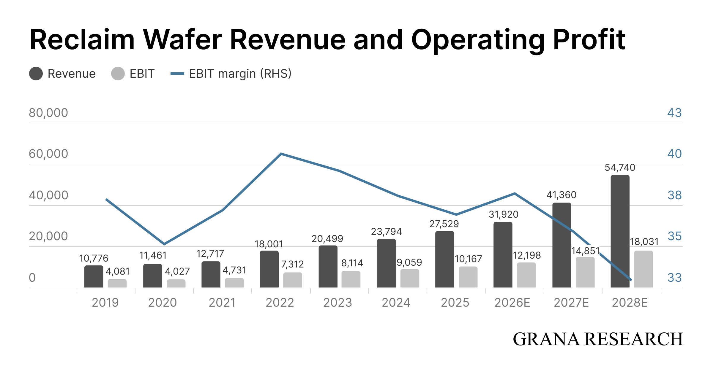
The wafer reclaim business is the company’s core segment, generating approximately 35% of revenue, 64% of operating profit (or roughly 75% excluding subsidies in the prime wafer segment), with operating margins in the high-thirties and ROIC above 20%. Both of the company’s key facilities (Japan and Taiwan) are currently operating at 100% utilization, running 24/7 across three shifts amid the AI-driven semiconductor boom. We expect segment revenue growth to accelerate from the current mid-teens to the high-twenties over the next several years, while operating profit could increase by approximately 77% between 2025 and 2028.
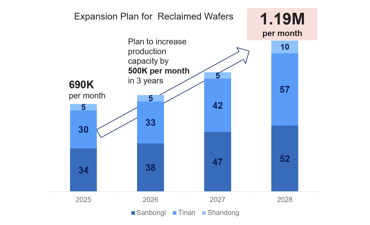
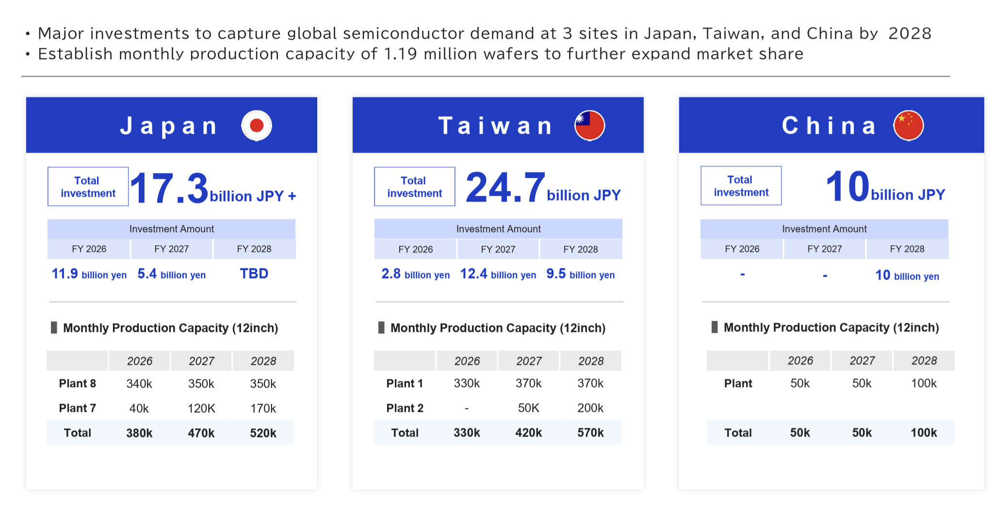
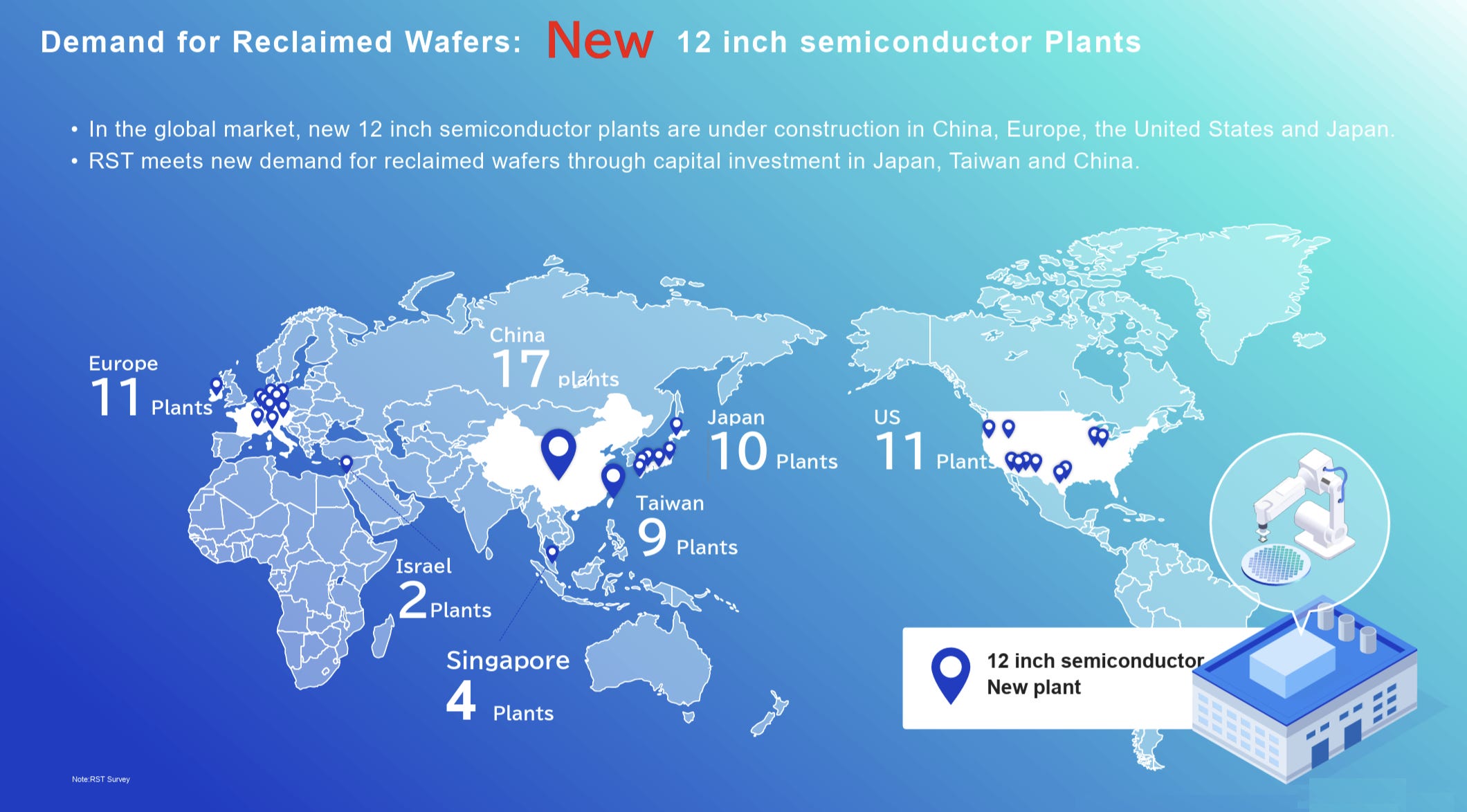
Demand is being supported by two structural tailwinds. The first is the construction of new fabs: more than 60 semiconductor fabs are currently under construction worldwide, including 11 in Japan and 9 in Taiwan, while TSMC has raised its 2026 CapEx guidance to $60-64 billion. The second is the migration toward leading-edge process technologies. Reclaimed wafer consumption intensity increases by roughly 3-4x for the same fab capacity (according to industry experts, from approximately 40k reclaim cycles per 50k wafer starts at 28nm to roughly 115k at 3nm and 135k at 2nm). To meet this demand, RST is investing ¥52 billion (~$324.6 million) to expand total reclaim capacity to 1.19 million wafers per month by 2028 (+72%), with Taiwan representing the primary expansion focus.
The prime wafer business (approximately 26% of revenue and 26% of operating profit) is entirely China-based and is consolidated through publicly listed GRITEK (688432 CH), in which RST holds an effective 39.1% economic interest. This business is capital-intensive, generates ROIC below 5%, and is only beginning to emerge from a prolonged industry downturn. Its long-term outlook remains mixed due to the structural transition from 200mm to 300mm wafers and aggressive pricing by Chinese competitors. However, GRITEK’s public listing makes the segment a key source of hidden value within the group.
Based on our model, we expect group revenue to grow at a 15.3% CAGR through 2028, operating profit at 19.5% CAGR, and net income at 19.8% CAGR, driven primarily by the increasing contribution of the higher-margin reclaim business. We forecast net income to exceed management guidance by 5%, 19%, and 23% in 2026, 2027, and 2028, respectively (management’s previous medium-term forecasts also proved conservative). While we expect free cash flow to remain deeply negative during the investment cycle, net debt should remain negative even if the entire expansion program is financed with debt.
We see two key risks. First, the company may gradually lose share at TSMC in the fastest-growing leading-edge nodes to Taiwanese competitor Phoenix Silicon International. Second, capital allocation remains a concern. While the core reclaim business is capacity-constrained and generates ROIC above 20%, management continues searching for a “second cash cow” by deploying capital into businesses earning only 3-5% returns, diluting the group’s overall return on invested capital.
Even after accounting for these risks, the valuation appears exceptionally attractive — both on conventional relative valuation metrics and on common sense. RST trades at a substantial discount to direct peers such as Phoenix Silicon (8028 TT), Kinik (1560 TT), and Scientech (3583 TT) despite offering comparable business quality and growth prospects. Moreover, RST’s 39.1% stake in publicly listed GRITEK alone was worth ~$2.9 billion as of July 29, while the entire market capitalization of RS Technologies stood at only ~$926.7 million. In other words, the market is effectively assigning a negative value to the company’s highly profitable and rapidly growing wafer reclaim business.
The Company
Semiconductor demand seemed inexhaustible. A technology that had once been confined to engineering departments and research laboratories suddenly became indispensable to virtually every product, every industry, and every economy aspiring to compete in the future. Capital poured into the sector. Companies raced to build new capacity, struggling to keep pace with incoming orders. An entire nation came to believe it held the key to the next technological era. Analysts spoke of a paradigm shift, newspapers wrote about the race for global leadership, and investors watched fortunes being created in real time.
This is not the story of today’s artificial intelligence boom. It is the story of Japan in the 1980s. It was during this period that Japanese memory manufacturers rose to dominate the global DRAM market, while demand for silicon — the industry's fundamental raw material — grew exponentially.
Against this backdrop, Japan's traditional industrial conglomerates began searching for entry points into this young and promising market. For Rasa Industries, historically a chemicals and materials company, the move into electronics was not a one-off bet but a long-term strategic transition. The company launched high-purity red phosphorus for electronics in 1972, entered the gallium market in 1981, and in January 1984 became the first company in Japan to enter the silicon wafer reclaim business, making it one of the industry's global pioneers [1].
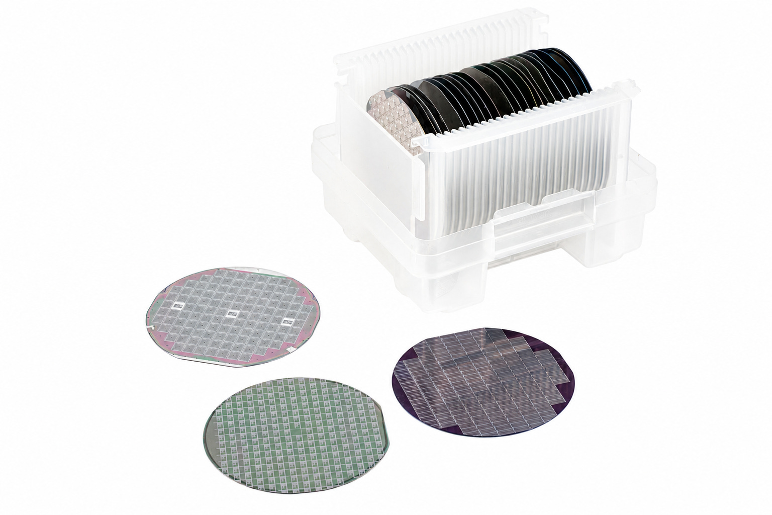
The economics of wafer reclaim are straightforward. Manufacturing semiconductor chips requires hundreds of process steps, with production quality verified at each stage using test wafers. Because prime wafers — the wafers ultimately used to manufacture chips — are expensive, it is far more economical to use reclaimed wafers for process monitoring.
By the early 2000s, the semiconductor industry was entering another transition. Following the prolonged downturn of the 1990s, chipmakers began migrating from 8-inch to 12-inch wafers (from 200 mm to 300 mm). The rationale was simple: larger wafers produce more dies per wafer, lowering the manufacturing cost of each chip. Between 2007 and 2008, Rasa invested approximately ¥5 billion to build a 12-inch wafer reclaim line with a capacity of roughly 100,000 wafers per month [2].
As is often the case in cyclical industries, timing proved unfortunate. The global financial crisis following the collapse of Lehman Brothers severely impacted semiconductor demand, fab utilization, and reclaim service pricing. In interviews conducted years later, RS Technologies' management described the situation candidly: Rasa was unable to absorb both the downturn and the burden of its recent investment, and in 2010 decided to exit the business altogether. The assets put up for sale included the Sanbongi wafer reclaim facility, along with its relatively new 12-inch reclaim production line.
It is at this point that Ho Nagayoshi — future founder, CEO, and largest shareholder of RS Technologies — enters the story. Ho was born in 1970 in China’s Jilin Province. His grandmother came from Japan’s Fukui Prefecture, making him a third-generation Japanese descendant. He moved to Japan in August 1988 at the age of sixteen, immediately after graduating from high school. After completing graduate studies in Japan, he founded Eiki Shoji in 1998, a company specializing in recycling and international trading of used computers, office equipment, and industrial machinery.
Eiki Shoji established a relationship with Intel: Intel’s irreclaimable silicon wafers, which had become waste, had to be disposed of, and Eiki Shoji purchased them for recycling — this marked its first connection to the wafer industry. When Rasa announced its exit from the business in 2010, Eiki Shoji became one of the bidders for the assets [4]. Three overseas buyers also competed for the assets. According to participants in the negotiations, they were willing to pay considerably more for the technology. Nevertheless, Ho’s group ultimately prevailed after committing to continue operations at the site, lease the factory from Rasa, and preserve manufacturing in Sanbongi [5].
Public sources are remarkably consistent regarding the economics of the transaction. Assets into which Rasa had invested an estimated ¥10-20 billion (~$125-250 million at the average 2011 exchange rate) were acquired for roughly ¥400 million — only $4.8-5.0 million [3].
Later, RS director Satoru Endo would say:
“It was a transfer made to facilitate Rasa’s exit after the Lehman shock, and for us it was a fortunate coincidence—we were able to start the business without bearing the burden of enormous capital expenditures.”
Under the terms of the transaction, only the equipment was transferred. The buildings at Sanbongi were leased, and 55 former Rasa employees who had been laid off were rehired. By that point, Rasa’s entire customer base had already moved to competitors, and the company started with zero revenue. Thus, RS Technologies was established in December 2010.
RS Technologies commenced operations in January 2011. However, in March, the Tohoku earthquake — the strongest in the country’s history, known as the Great East Japan Earthquake — struck. The company was able to reach the break-even point only in the second half of 2012 [6].
The company’s next step was expansion into Taiwan. Ho personally went to TSMC to offer reclaimed wafers. However, TSMC’s position was firm: the product quality was good, but the delivery cycle was too long — three weeks; if it could be reduced to two weeks, they could begin discussing orders. In February 2014, RS established its Taiwanese subsidiary, and in December 2015 completed its factory in Tainan. In its 2015 presentations, the company stated that the new Taiwanese facility had an initial capacity of 100,000 12-inch wafers per month. The company also became publicly listed that same year.
In March 2015, RS went public; in June 2015, it completed the eighth building at its Sanbongi plant, and following the IPO, it began rapidly expanding capacity. Toyo Keizai writes that in 2015 alone, the company invested a total of ¥7.7 billion (~$63-64 million) in the reorganization and expansion of the Sanbongi facility and in the construction of its new factory in Taiwan [7].
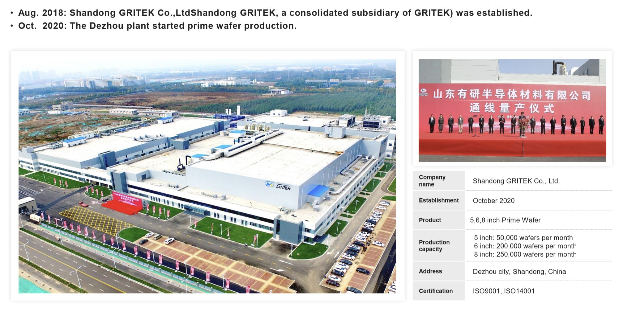
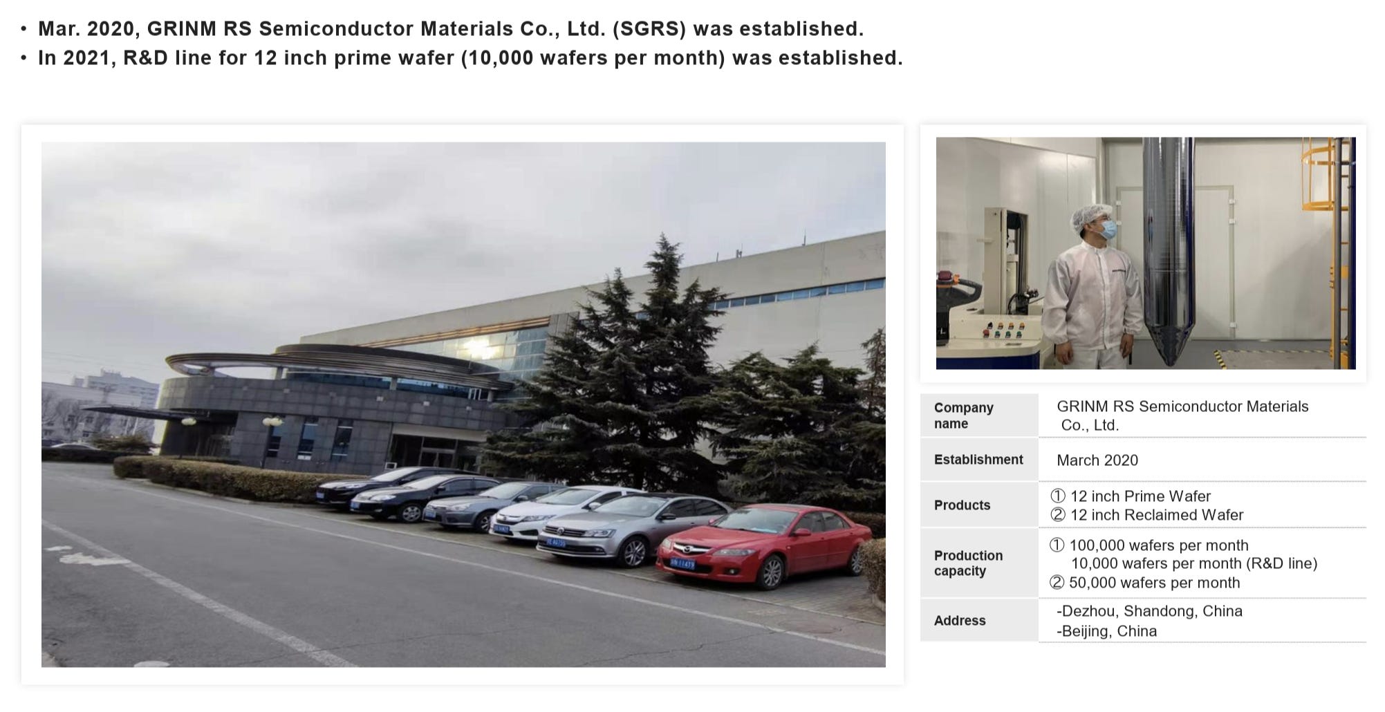
The second strategic turning point was the company’s entry into the prime wafer market. In December 2017, RS signed a joint venture agreement with China’s GRINM and Fujian Cangyuan, allowing it to enter the prime wafer market for the first time. Shandong GRITEK manufactures and sells 5-, 6-, and 8-inch wafers (125, 150, and 200 mm), and since 2020, through the SGRS joint venture, has been conducting research and development aimed at the mass production of 12-inch (300 mm) wafers.
At the same time, RS began assembling a broader portfolio of assets, including a business manufacturing quartz glass components and parts, the distribution of power semiconductors, the production of electrolyte for vanadium redox flow batteries, and other businesses.
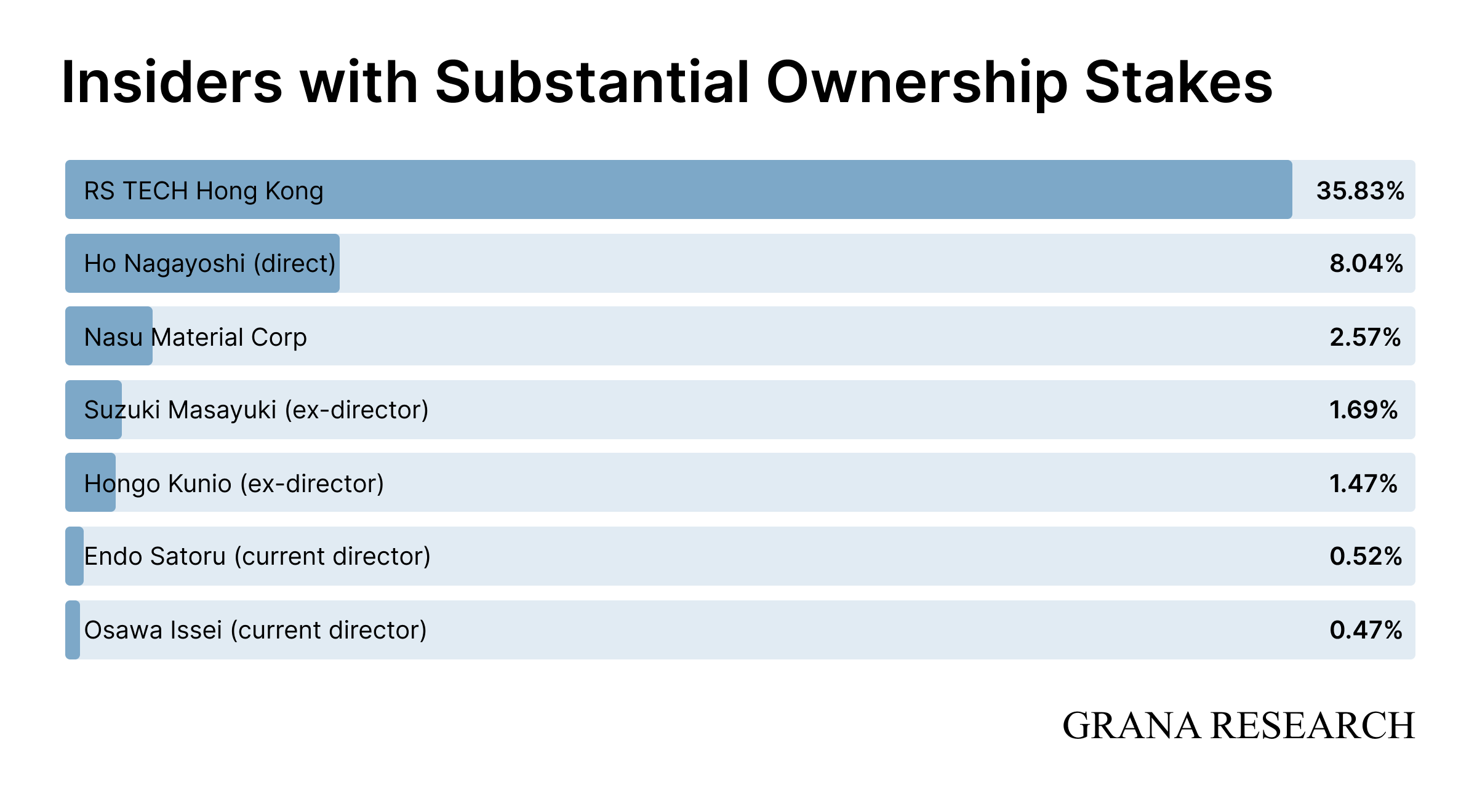
Today, RS Technologies is one of the leaders in the small, capital-intensive, yet critically important silicon wafer reclaim market, with a broad portfolio of additional assets. Ho Nagayoshi remains the company’s CEO and controlling shareholder, owning 43.87% of the shares (8.04% directly and 35.83% through RS TECH Hong Kong). In total, insiders and affiliated parties own 50.59% of the company.
Wafer Reclaim Business (~35% of Revenue and ~64% of Operating Profit)
Two types of silicon wafers are used in semiconductor manufacturing: prime wafers and test wafers. Prime wafers are the highest-quality silicon substrates, manufactured from single-crystal silicon and intended for the fabrication of integrated circuits, processors, and memory chips. Test wafers are consumable silicon substrates used at semiconductor fabs such as TSMC, GlobalFoundries, and Intel for equipment qualification, process monitoring, and experimentation.
After use, a test wafer is not discarded but reclaimed and reused. Following a process run, the wafer is covered with process films, contaminants, and microscopic defects — but if these are carefully removed, the wafer becomes suitable for reuse. According to RS Technologies, test wafers account for about 20% of all wafers used in semiconductor manufacturing, and roughly 80% of them are reclaimed wafers. Each wafer can typically go through the reclaim process up to approximately ten times before it becomes too thin and must be scrapped.
Fabs prefer reclaimed wafers because they are significantly less expensive than new ones. According to a Former Manager at GlobalFoundries, a reclaimed wafer costs $20-30 per wafer, compared with around $100 for a new one [20]. A Former Manager at Phoenix Silicon, RS Technologies’ main competitor, provides a similar estimate:
Interviewer
Do you know the pricing, how much it costs for one wafer reclaim cycle for each of these nanometers?”
Former Manager at Phoenix Silicon
The business department is definitely more in charge of the pricing. The exact numbers are company trade secrets. I can provide you some ranges. In general, the wafer reclaim price is 1/3 of the prime wafer price. It will change depending on some factors including the particle size requirement, the outer volume by that customer. Those things will change the actual price.
Interviewer
What would you categorize as the price of a prime wafer here?
Former Manager at Phoenix Silicon
In general, a prime wafer costs $100-$120, but if we’re looking at the really advanced nodes it will be quite a bit more expensive. Based on publicly available information, I believe those more advanced process wafers are two to three times as expensive as the general wafer price.
In some cases, reclaimers purchase wafers outright and resell them after cleaning. However, the majority of revenue is generated under a service model. Ownership of the wafer remains with the customer, while RS earns revenue by providing the reclaim service. The reclaim process is as follows:
Shipment. The fab collects used test wafers and ships them to the reclaim supplier in batches.
Incoming inspection and sorting. The wafers are classified by diameter, film type, and degree of wear, as some are already unsuitable for reclaim because they have become too thin. At this stage, 10-20% of the wafers are rejected.
Film removal and wet cleaning. Deposited films and contaminants are removed through chemical cleaning.
Chemical Mechanical Planarization (CMP). The wafer surface is restored to a condition comparable to that of a new wafer while maintaining geometry and thickness within specification.
Final inspection and return to the customer. For high-grade wafers, the reclaim yield is typically 80-90%. For medium-grade wafers, it is 70-85%, while for mechanical-grade wafers, it is 60-75%.
When the fab and the reclaim supplier are located nearby, the entire cycle — from sorting to return — typically takes 1–2 weeks. With regional transportation (for example, Taiwan to Japan), the cycle extends to 3-4 weeks, with logistics costs of ~$2-4 per wafer. Intercontinental shipments (for example, the U.S. to Asia) take 6-8 weeks and add roughly $8-10 per wafer in logistics costs.
Lead time and logistics are important considerations for customers. While wafers are in transit and undergoing the reclaim process, they remain tied up in the supply chain, requiring customers to maintain buffer inventory throughout the entire cycle. This represents additional working capital tied up in inventory. This is likely what explains TSMC’s firm stance on delivery cycle time. As one Consultant in Semiconductor Wafer explains:
“When you do the wafer reclaim... there’s a lot of wafer accumulated in the whole supply chain. In RS Technologies from door-to-door means day one leave the TSMC door until the day that arrive TSMC door again, it takes around like three to four weeks... It means on average sent to RS Technologies, you accumulate four weeks wafer volume in the supply chain. It means money. However, if you use [a local supplier], it takes around just one week. Four weeks versus one week, the money accumulated right there is significant, especially when TSMC is big enough.”
Wafer Reclaim is the core business of RS Technologies, accounting for ~35% of revenue and ~64% of operating profit (or ~75% of operating profit excluding subsidies received by the Prime Wafers segment). The company’s production capacity is distributed as follows:
Sanbongi Plant (Japan)
8-inch: 150,000 wafers/month;
12-inch: 340,000 wafers/month;
Planned to increase capacity to 520,000 wafers per month (+53%) by 2028.
Tainan Plant (Taiwan) – operated through the subsidiary RSTEC Semiconductor Taiwan
12-inch: 300,000 wafers per month;
Planned to increase capacity to 570,000 wafers per month (+90%) by 2028.
China Plant
12-inch: 50,000 wafers per month;
Planned to increase capacity to 100,000 wafers per month (+100%) by 2028.
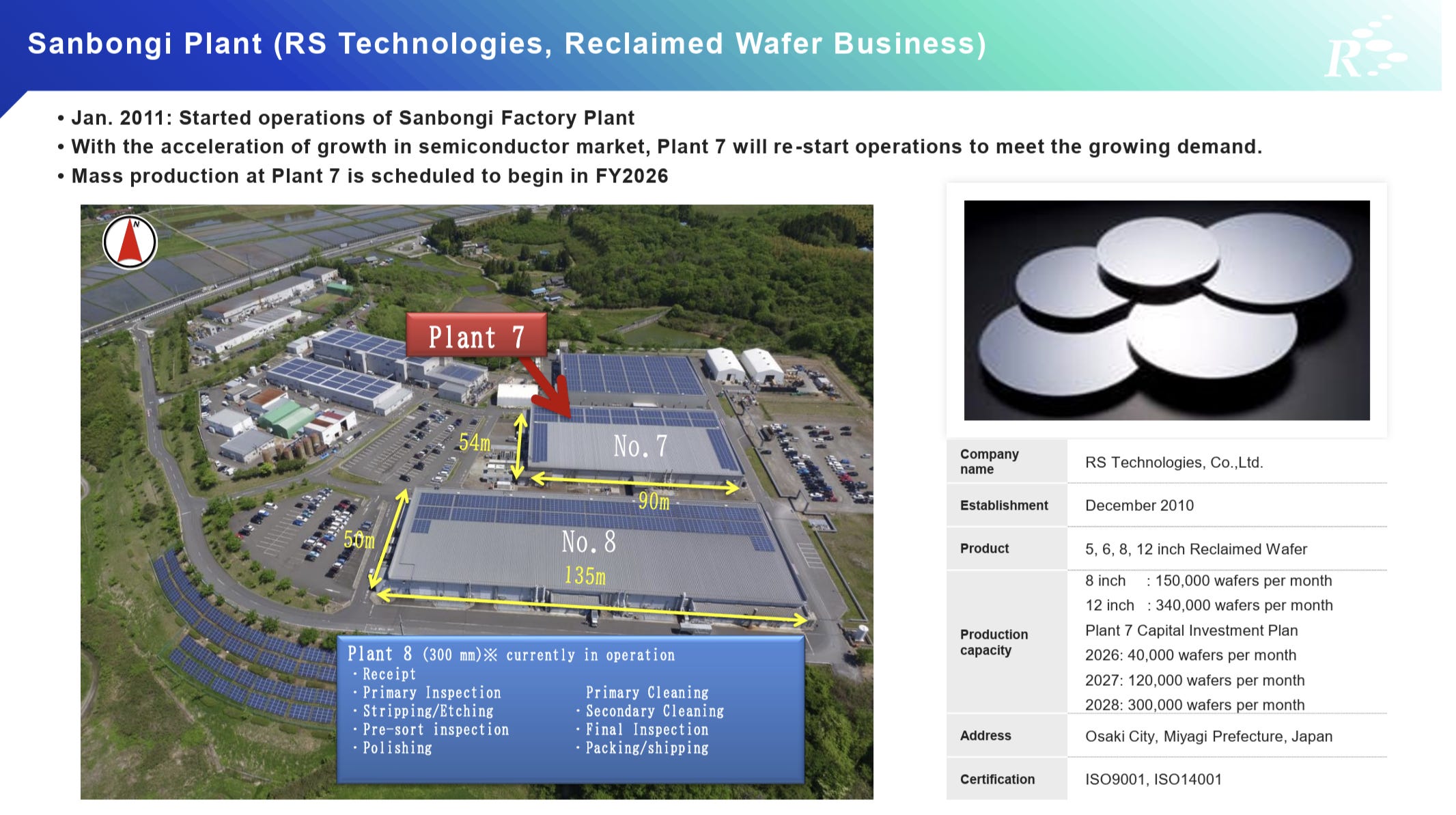
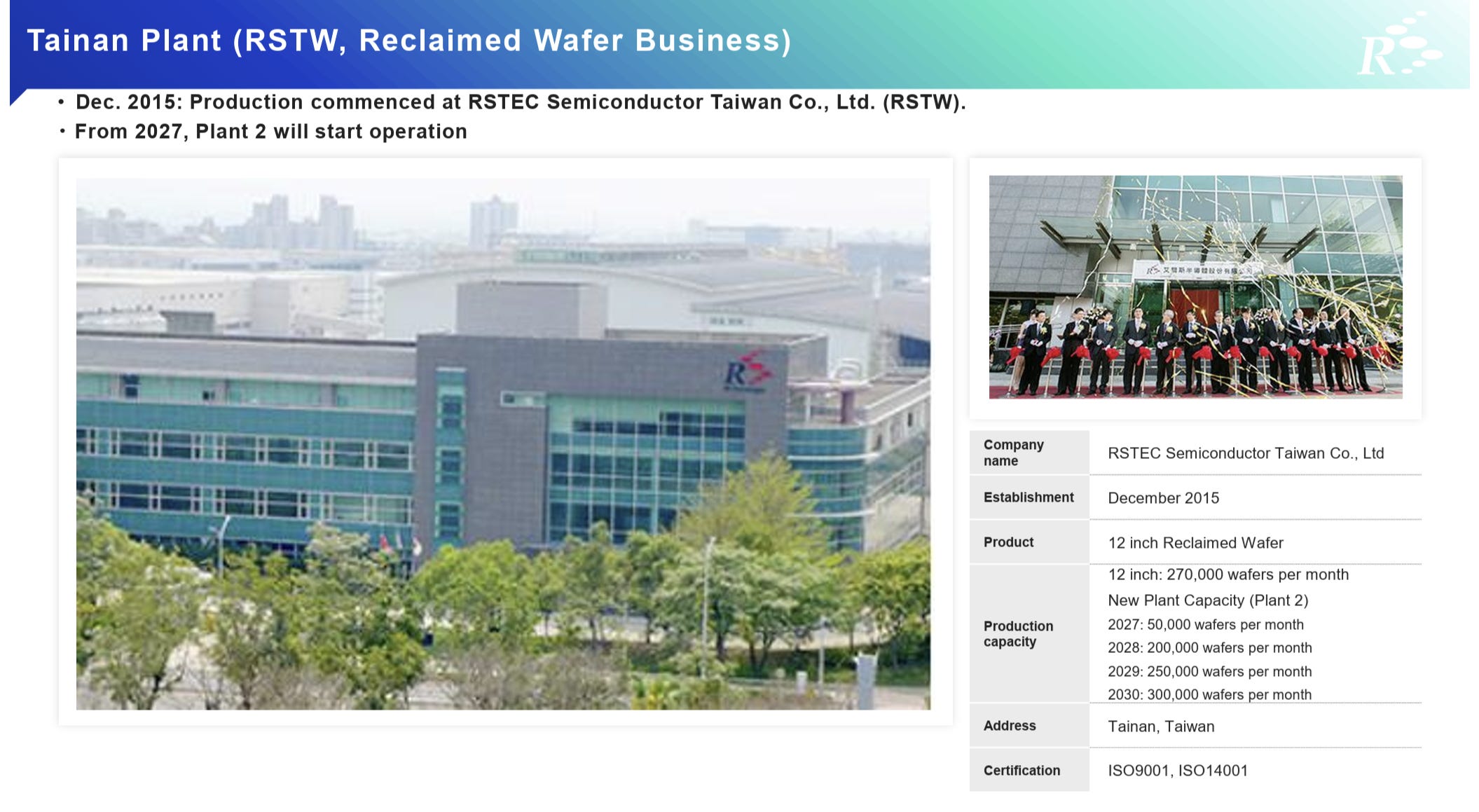
According to management, both the Japan and Taiwan plants are operating at 100% utilization due to the AI boom. Moreover, the company has stated that there are periods when the facilities have no available capacity at all, operating 24 hours a day in three shifts. As a result, RS Technologies is forced to turn away customers — indicating not only full utilization, but also unmet demand.
RS Technologies plans to invest ¥52 billion (~$324.6 million) in these facilities to increase their combined monthly capacity to 1.19 million wafers by 2028. Notably, the expansion in Taiwan will be more aggressive, which is particularly important in the context of supply chain localization for TSMC.
The segment has two key customers: Sony (~20% of the group’s total revenue) and TSMC (~18%). Together, they account for the vast majority of the company’s wafer reclaim revenue.
The wafer reclaim market is a small oligopolistic market, with the four largest players controlling about 70% of global capacity. RS Technologies is one of these market leaders, with management estimating its market share at approximately 31%. However, based on our analysis, the company’s actual market share may be lower, as discussed in the Risk Factors section.
It is also worth noting that several industry experts describe the wafer reclaim business as countercyclical, since monitor wafers and dummy wafers are essential consumables required to maintain manufacturing yield, regardless of end-market chip demand.
Within its Wafer Reclaim business, the company has two key growth drivers: first, the construction of new semiconductor fabs around the world; and second, the transition to more advanced process nodes.
New Semiconductor Fabs Worldwide
Every new semiconductor fab represents a new, structural source of demand for both new and reclaimed wafers. According to RS Technologies, more than 60 new fabs are currently under construction worldwide, including 11 in Japan and 9 in Taiwan.
Against the backdrop of the AI boom, capital expenditures across the industry continue to accelerate. In January 2026, TSMC raised its full-year capital expenditure guidance to $52-56 billion, up from $40.9 billion the previous year, and following its most recent earnings report, increased the guidance further to $60-64 billion. According to Goldman Sachs, TSMC’s manufacturing capacity is expected to expand by approximately 25% by the end of 2028 [21].
Memory manufacturers are also expanding capacity aggressively in response to the severe supply shortage. According to Barclays, total DRAM wafer supply is expected to increase by ~70% by 2030, implying a CAGR of ~11%. These projections are indirectly supported by Sumco, one of the world’s largest manufacturers of prime wafers, which forecasts demand for 12-inch wafers to reach 10 million wafers per month by 2028. For comparison, demand stood at 7.8 million wafers per month in Q1 2026 [9].
On May 8, 2026, Sony and TSMC signed a memorandum of understanding to establish a strategic partnership for the development and manufacturing of next-generation image sensors. Most of the new production capacity will be deployed at the new fab currently under construction in Koshi, Kumamoto Prefecture, Japan. Sony will hold a majority and controlling stake in the joint venture.
The JASM Phase 1 and Phase 2 (Japan Advanced Semiconductor Manufacturing) facilities are expected to support process nodes ranging from 40nm to the leading-edge 3nm node. Combined production capacity will reach approximately 100,000 wafers per month. Given the proximity of RS Technologies’ operations, the company is likely to capture the largest share of wallet from this project.
Transition to More Advanced Process Nodes
For those familiar with TSMC, it is no secret that with each new generation of chips, the company seeks to increase the number of transistors that can be integrated onto a single wafer. This is known as process node scaling in accordance with Moore’s Law, while the progression from one generation to the next is referred to as the transition to more advanced process nodes (advanced nodes).
Historically, this progress was measured in nanometers, which once reflected the actual physical dimensions of a transistor’s gate. Today, these figures have largely become commercial generation labels, but the underlying engineering challenges remain fundamentally the same.
Today, the most advanced process nodes (7nm, 5nm, and 3nm) account for 39% of TSMC’s manufacturing capacity and 74% of its revenue. The share of advanced nodes is expected to exceed 60% of total capacity by the end of 2028.
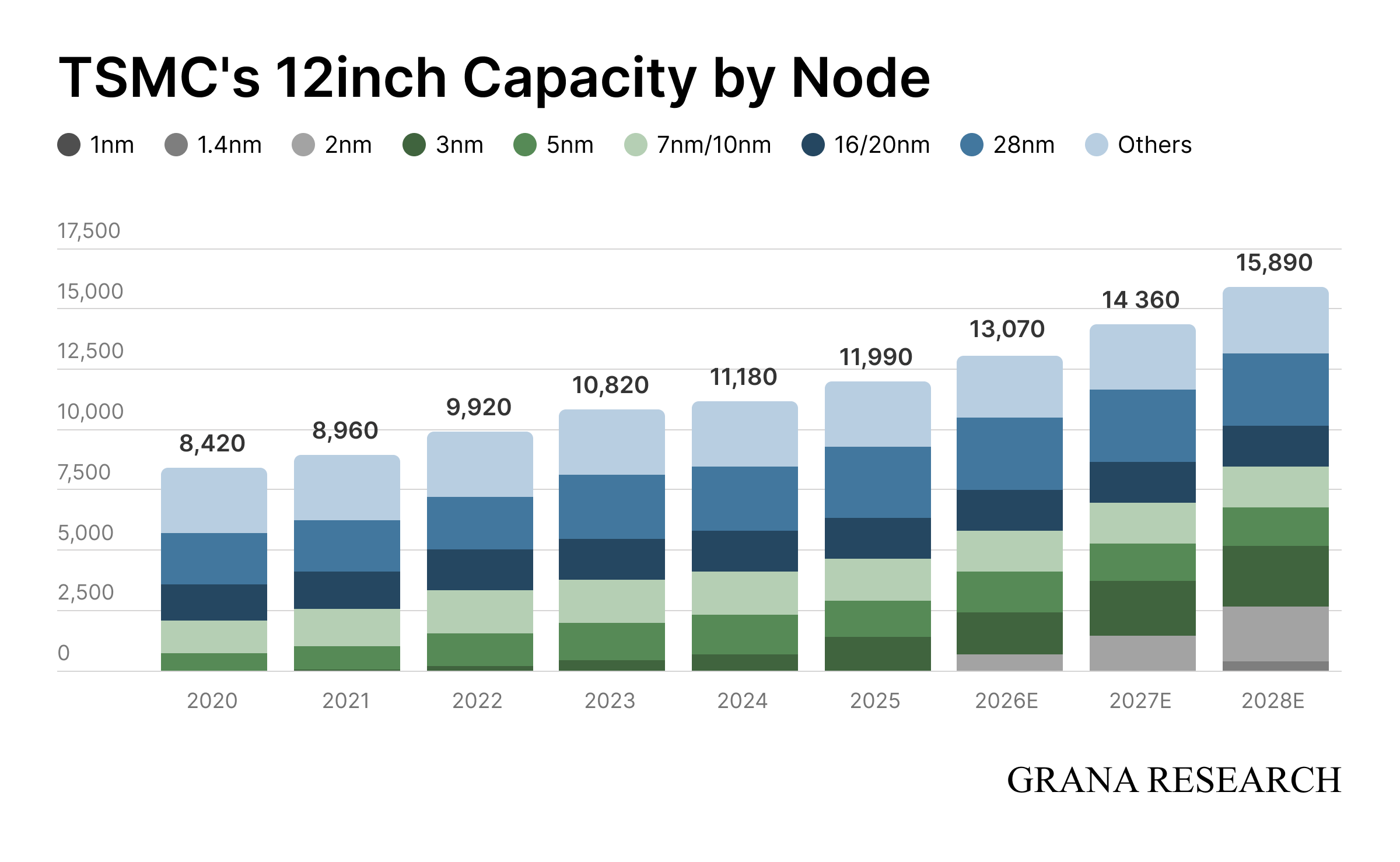
The transition to more advanced process nodes is a key driver of demand for reclaimed wafers, because as transistor density increases, the number of lithography, etching, and deposition steps also rises, along with the number of test, monitor, and dummy wafers required for each production wafer. In other words, demand for wafer reclaim increases even without the construction of new fabs, simply as a result of migration to more advanced process nodes.
The scale of this effect is illustrated by a Former Manager at Phoenix Silicon. According to the manager, the intensity of reclaimed wafer usage increases significantly as fabs transition to more advanced process nodes, even when fab capacity remains unchanged.
Interviewer
Let’s see. In terms of the overall demand for wafer reclaim, let’s say you have a fab doing 50,000 wafer starts per month. How much wafer reclaim demand are you going to have? I think this was one of the questions but breaking it out by nanometer as well would be helpful.
Former Manager at Phoenix Silicon
I’m not that involved in capacity planning. I can just give you some rough numbers. For 28 nm, if the wafer start number is 50,000 per month, then we will need 40,000 reclaim wafer. However, that doesn’t mean the absolute number of reclaim wafers we will be using because each wafer can be reclaimed five to 10 times.
If we divide that 40,000 by 10, the actual reclaim wafer that will be used in that month will be 4,000 pieces.
However, they need to perform wafer reclaim for 40,000 times to be able to meet the requirement. For three nm, for the same capacity, we will use the wafer reclaim process for 115,000 times. For the two nm, there is a rough calculation. They suspect in the future, we will use 135,000 times of the wafer reclaim.
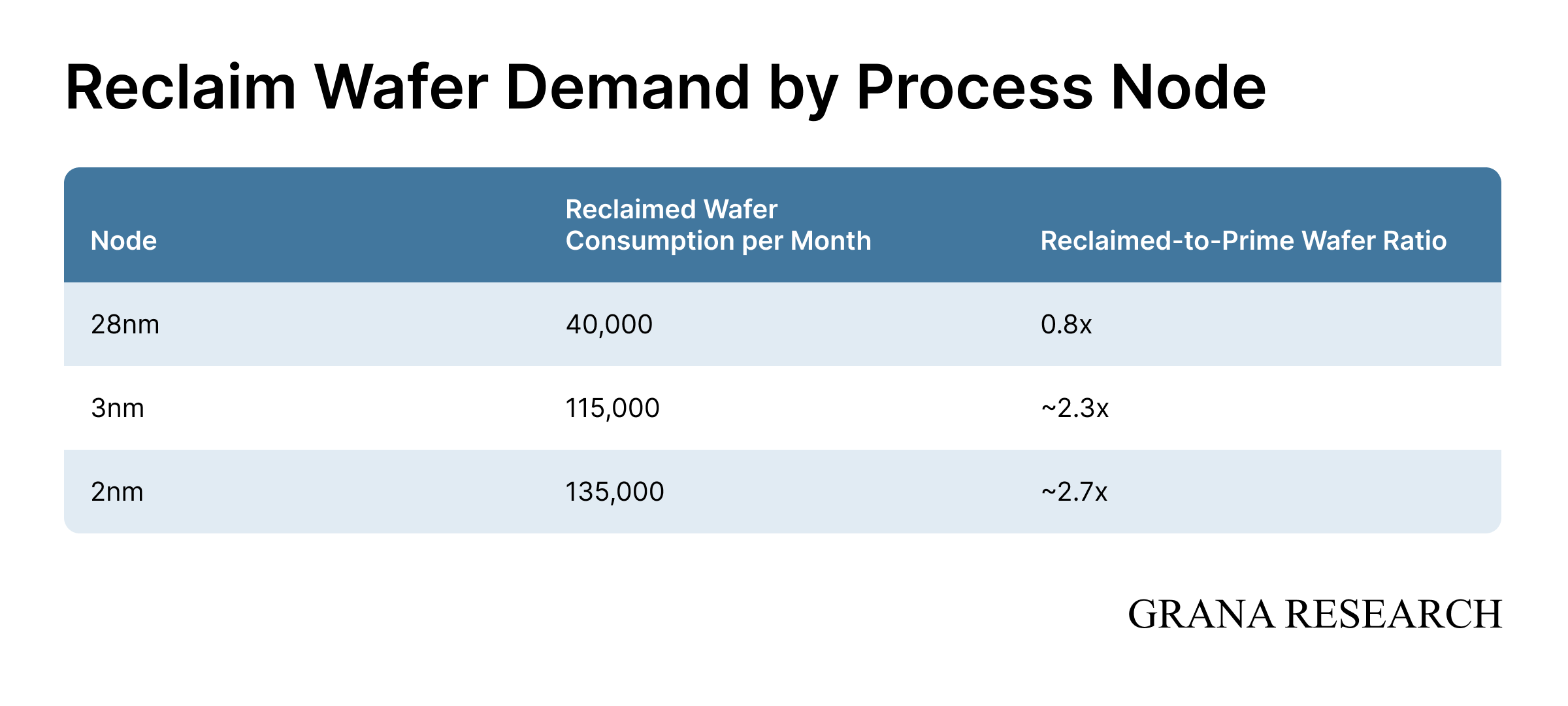
According to a Consultant in Semiconductor Wafer, the transition to more advanced process nodes can increase demand for reclaimed wafers by 3-4x, even with the fab’s manufacturing capacity remaining unchanged:
Interviewer
Just on the advanced nodes for TSMC, can you talk me through the shift to advanced node and what the impact is on the reclaim business? Obviously, the understanding is because its more advanced node the dummy ratio or the test wafer ratio is going to be higher, there’s more wastage.
Consultant in Semiconductor Wafer
Yes, I have a number.
Interviewer
Yes, this is obviously positive for the volume of reclaim. I just wanted to understand, is it more the benefit for reclaim? Is it more that it’s a higher dummy ratio or more that the percent of dummy ratio that is reclaimed is higher? Is it both?
Consultant in Semiconductor Wafer
Let me share the number with you. All the data are for 12-inch. Every 1,000 product wafers, they need 600 dummy wafers and monitor wafers. If we combine everything into like every 1,000 require 600 for the reclaimed wafer. However, when we move to the 28 nm, every 1,000 requires around 1,500-2,000 reclaimed wafers. The ratio from one to 1.6, 1.5 to 2.0.
When you move to the like five nm, it can move to more than 1,000-2,500, which means every 1,000 product wafer you require like 2,500 recurring wafers, which means even TSMC do not establish the new fab but their technology should not keep migrating from 65 nm to 28 nm to seven nm.
Even the same fact of 50,000 wafer per month capacity, the recurring way the recurring wafer demand increase three to four times easy. This is the power of the migration. Meanwhile TSMC keep building the new fab as you know, so two factors multiplied together.
The phrase “two factors multiplied together” neatly captures the essence of the investment thesis: migration to advanced process nodes, which require 3-4x more reclaimed wafers per fab, is compounded by the growing number of semiconductor fabs being built worldwide. This shift in the industry mix toward advanced nodes is precisely the growth driver behind RS Technologies’ plan to expand its reclaim capacity by 72% by 2028. According to management, the company’s capacity expansion investments have been coordinated with its customers’ production plans.
Prime Wafer Business (~26% of Revenue and ~26% of Operating Profit)
If reclaimed wafers are the semiconductor fab’s consumable, then a prime wafer is the monocrystalline silicon substrate on which integrated circuits are actually built. Its journey begins with the growth of a single-crystal silicon ingot using the Czochralski process. The ingot is then sliced into wafers, ground, mirror-polished, and, where required, an epitaxial layer is deposited. The entire manufacturing process — from crystal growth to the packaging of finished wafers — is well illustrated in the following video.
The 12-inch (300 mm) wafer segment accounts for the majority of the market — approximately 75% by value. These wafers are used primarily in the production of logic and memory chips. 8-inch and smaller wafers (5-, 6-, and 8-inch, or 125 mm, 150 mm, and 200 mm) are primarily used for power semiconductors, analog integrated circuits, discrete devices, and sensors.
RS Technologies entered the prime wafer market in 2018 through a joint venture with the Chinese state-owned General Research Institute for Nonferrous Metals (GRINM). A special-purpose vehicle, Beijing GRINM RS Semiconductor Technology Co., Ltd. (BGRS), was established. BGRS owns a 30.8% stake in the publicly listed GRITEK (Ticker: 688432 CH), which in turn owns 85% of the operating company Shandong GRITEK.
RS Technologies owns 45% of BGRS and a 25.2% stake in publicly listed GRITEK directly. As a result, RS Technologies’ effective ownership interest in GRITEK is 39.1% (25.2% direct ownership plus 13.9% indirect ownership through BGRS).
Although RS Technologies’ total economic interest is 39.1%, the company controls GRITEK and therefore consolidates its financial results. RS Technologies paid ~$47 million for its 45% stake in BGRS. The ownership structure also includes Fujian Kuramoto, a company affiliated with Ho Nagayoshi.
This complex ownership structure serves a single purpose: to ensure that the Chinese business is treated as a domestic enterprise and therefore qualifies for Chinese government subsidies. It is worth noting that these subsidies account for approximately 13% of GRITEK’s ordinary income [11].
A separate joint venture, Shandong GRINM RS Semiconductor Materials Co., Ltd. (SGRS), was established for the 12-inch (300 mm) wafer business, in which the publicly listed GRITEK holds a 28% stake. As a result, RS Technologies’ effective economic interest in the 12-inch prime wafer business is 11.2%.
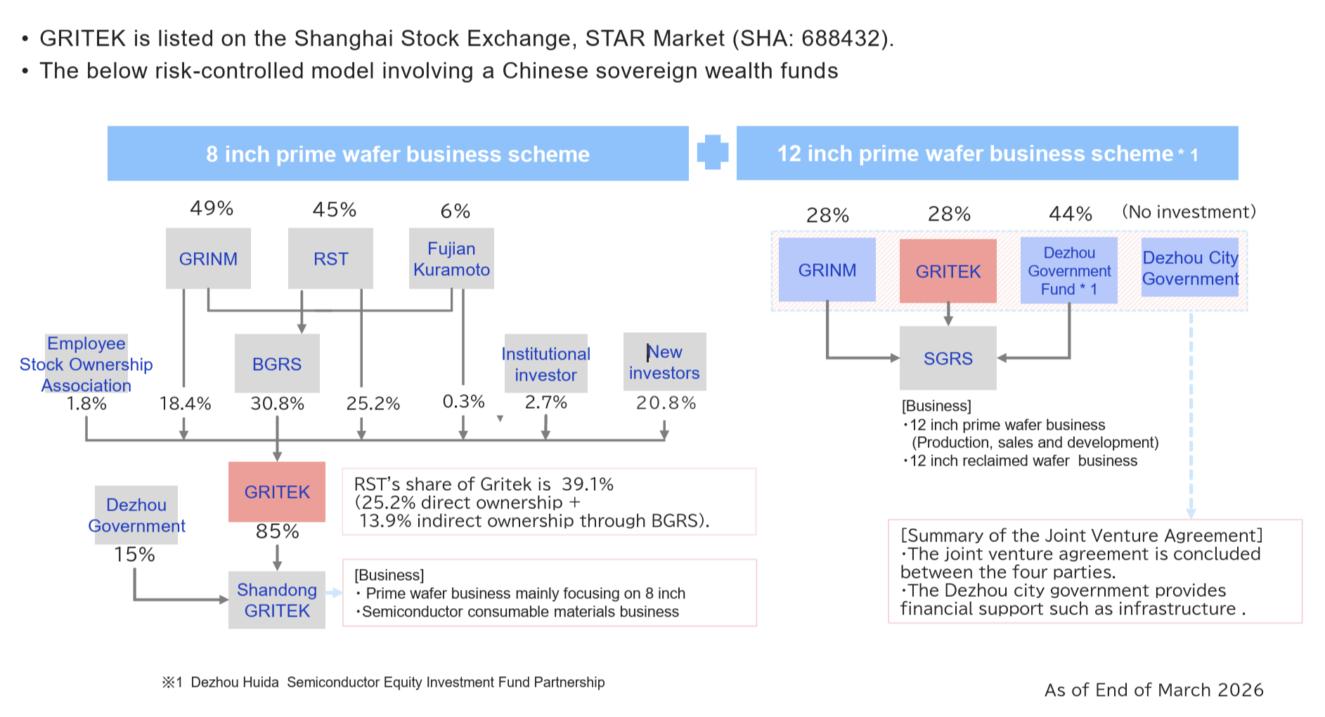
Within the segment, 56% of revenue is generated by sales of 5-, 6-, and 8-inch prime wafers. The production capacity is distributed as follows:
5-inch: 50,000 wafers/month;
6-inch: 200,000 wafers/month;
8-inch: 250,000 wafers/month.
Approximately 32% of segment revenue comes from silicon components, including consumable parts used in wafer etching equipment — such as shower plates, polycrystalline silicon rings, focus rings, and other silicon components used to distribute process gases, control plasma, and ensure etch uniformity. These components are gradually eroded during operation and must be replaced regularly, creating a recurring revenue stream tied to semiconductor fabs’ capacity utilization.
A further 12% of revenue comes from sales of complete silicon ingots used to manufacture wafers, including ingots produced using the float-zone process.
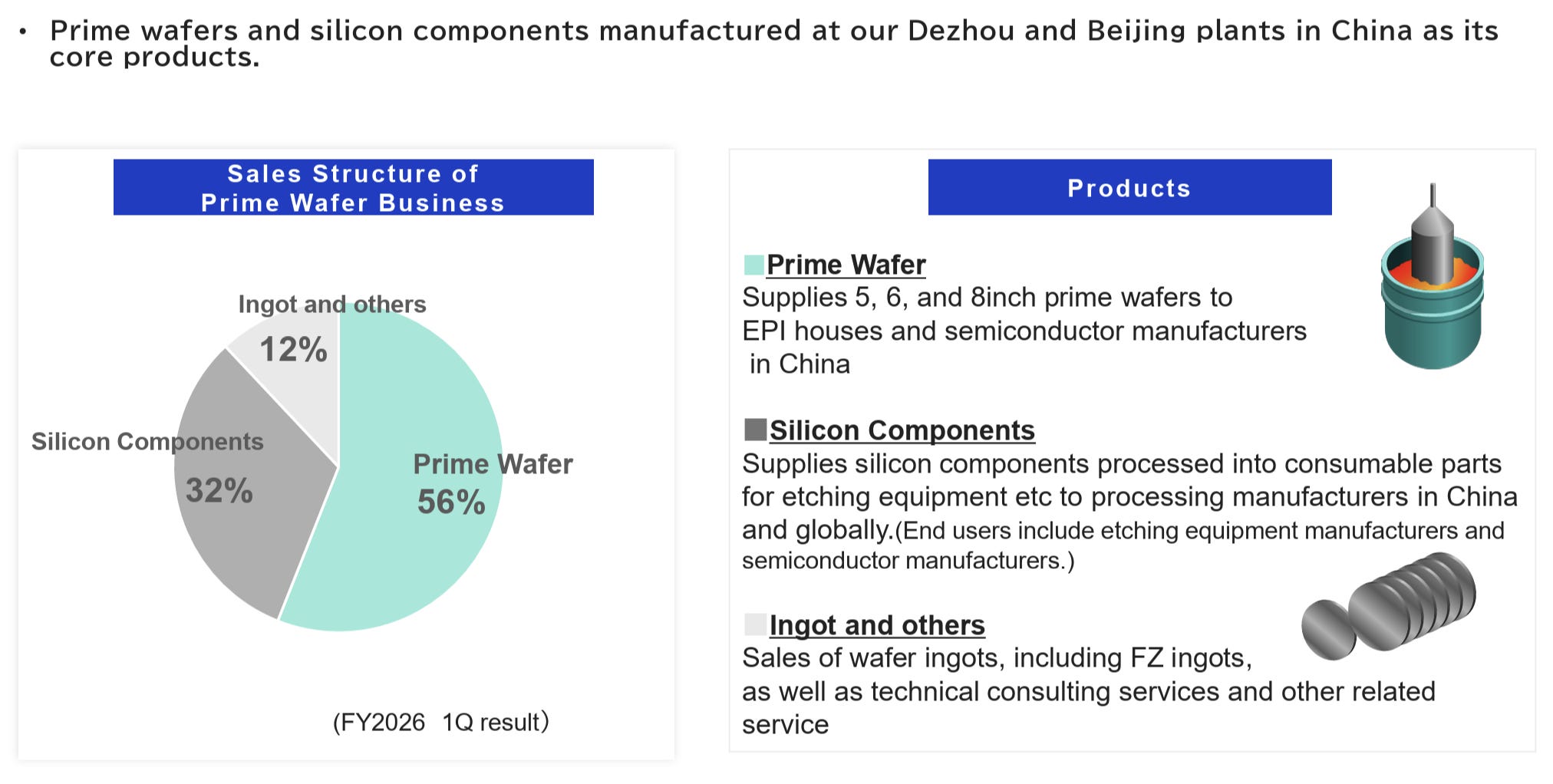
In our view, the outlook for this business is mixed. On the one hand, China continues to aggressively promote the localization of its semiconductor supply chain. For example, the government supports the adoption of domestically produced wafers even when their yield is lower than that of international competitors, fully compensating chip manufacturers for the resulting losses.
On the other hand, the silicon wafer industry has experienced a deep cyclical downturn globally in recent years. While demand for 12-inch wafers has begun to recover amid the current boom in advanced process nodes, the recovery in the mature-node segment (consumer and industrial electronics) remains weak, with wafer prices continuing to decline due to the persistent imbalance between supply and demand. Customers are also continuing to normalize 8-inch wafer inventory levels.
The situation is further complicated by the ongoing migration of many semiconductor manufacturers from 8-inch to 12-inch wafers. A 12-inch wafer has 2.25x the surface area of an 8-inch wafer, while processing costs are only 1.3-1.5x higher. As a result, the cost per die declines by ~30-40% following the transition.
Fabs built during the 1990s and 2000s continue to use 8-inch wafers because their manufacturing equipment was designed for that wafer size, while the cost of converting an entire fab exceeds the potential savings achieved on a per-die basis. However, as older manufacturing capacity is retired, the transition to 12-inch wafers is expected to continue.
In the West, this transition began many years ago, with demand for 12-inch wafers surpassing demand for 8-inch wafers as early as 2007 [12]. Companies such as Texas Instruments are targeting 80% of production on 12-inch wafers by 2030 [13]. Today, measured by total wafer surface area, 8-inch wafers account for only around 20% of the global market.
Similar trends are evident in China. For example, at SMIC, the country’s largest foundry, more than 80% of revenue is generated from 12-inch wafers. Nexchip, UNT, Silan, and CR Micro are also actively expanding 12-inch capacity for the production of analog and power semiconductors [20].
Against this backdrop, the following comments from SUMCO’s management during the Q2 2025 earnings call are particularly noteworthy:
“The trend reflects the combination of this China impact as well as the fading of demand for 200-millimeter wafers. The fading of demand is the result of weaker economic conditions as well as the transitioning of some applications to 300-millimeter wafers. The fall in demand as a result of weaker macro conditions should recover when economic conditions improve. But as the loss of demand on the back of applications transitioning to 300-millimeter represents a structural change, demand here will not come back.”
Also noteworthy are the comments from the Chief Commercial Officer of NSIG, China’s largest silicon wafer manufacturer, which accounts for ~6% of the global market:
Local competition from China for the power application part also for the logic part, I think other parties, they’re transition into 300 mm, especially in China. There’s been quicker transition to 300 mm than it was expected in this power and legacy market area. Even, let’s say, 2021, it was still expected that it’s much lower, the speed of the transition. Even some of the processes that it’s not expected to be transferred to 300 mm, but it has happened quicker especially there in China, also in Europe, and with some of the U.S. players too.
In Taiwan, for example, TSMC’s even talking about reducing the 200 mm, totally cutting down closing the 150-mm line but reducing 200 mm manufacturing space and this way, also volume. That’s affecting the transition for the volumes and the China local suppliers. I think these are two very important elements there. There have been rumors about that some of these big players are even cutting shutting down some of their 200 mm manufacturing capabilities factories.
I have not heard anything specific related to SUMCO on this field. If you look at the public numbers for the 200-mm manufacturing, it is lower than it used to be. In most of this data, China players are still missing. Missing the data from the China players, but the trend is not upwards. Also, I think that’s what SEMI forecasted, organization for semiconductors. The 200 mm will be in the lower growth percentages than the 300 mm.
RST/GRITEK’s management also recognizes the structural importance of 12-inch wafers. The company forecasts that demand will increase from 2.5-2.6 million wafers per month today to 4 million per month by 2030, with RST targeting a 7% market share. In 2026, the company plans to invest ¥3.80 billion ($23.95 million) to expand 8-inch wafer production capacity to 300,000 wafers per month, as well as ¥8.0 billion ($50.4 million) to increase 12-inch wafer capacity to 150,000 wafers per month. In 2027, it plans to further expand 12-inch capacity to 250,000-300,000 wafers per month, investing a substantial ¥17 billion ($107.2 million).
Investments in China are primarily made through the establishment and recapitalization of joint ventures in which RST holds ownership stakes.
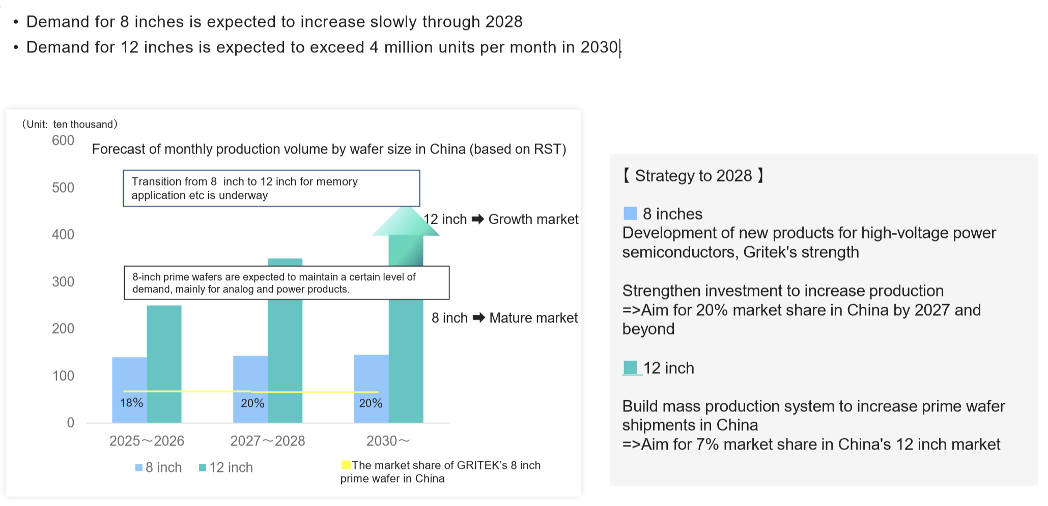
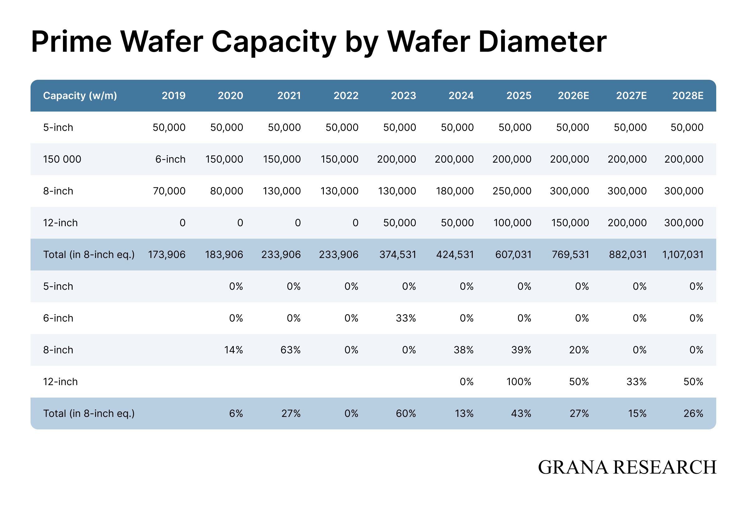
RS Technologies’ prime wafer segment is a capital-intensive business whose core production assets are subject to ongoing technological obsolescence. As substrate requirements for cleanliness, flatness, and defect density become increasingly stringent with each successive process node, maintaining competitiveness alone requires continuous reinvestment. At the same time, the structural growth in demand within China is unevenly distributed. It is concentrated in the 12-inch segment serving advanced logic and memory, whereas GRITEK’s prime wafer business is focused on the 8-inch segment, where unit prices remain under structural pressure. To capture the faster-growing portion of demand, RST is forced to invest in the 12-inch business through SGRS, which has yet to enter mass production and is currently loss-making. Meanwhile, Chinese wafer manufacturers are aggressively competing on price while simultaneously shifting their own production from 8-inch to 12-inch wafers.
Assessing the potential and quality of this business is ultimately a matter of debate. Nevertheless, the prime wafer business represents an important part of the RS Technologies investment thesis. As noted earlier, GRITEK is a publicly listed company trading under ticker 688432 on the STAR Market of the Shanghai Stock Exchange. As of July 29, 2026, GRITEK’s market capitalization stood at RMB 49.86 billion (~$7.36 billion). Accordingly, RS Technologies’ 39.1% stake is worth ~$2.9 billion, while RST itself is valued at only $926.7 million.
It is worth noting that following GRITEK’s IPO on the STAR Market, RST became subject to a 36-month lock-up period. In Q1 2026, RS Technologies reduced its ownership stake by 1%, selling shares in the open market. We spoke with the company’s Investor Relations team. According to management, they recognize the company’s undervaluation and understand the levers available to unlock shareholder value.
Semiconductor-related Equipment & Materials Business (~39% of Revenue and ~10% of Operating Profit)
This is the company’s most heterogeneous segment, assembled through a series of M&A transactions. While it is formally the largest segment by revenue, it contributes only around 10% of operating profit.
The largest subsegment by revenue is RS Precision Device Huizhou (RSPDH), the Chinese business manufacturing optical pickup modules and in-vehicle camera modules, acquired from Sony in the fall of 2024. In 2025, this business accounted for 50% of segment revenue.
The second-largest business is DG Technologies, a manufacturer of consumable components for wafer etching equipment, acquired in 2019. The third is Union Electronics, a distribution company supplying Minebea power semiconductors and Renesas microcontrollers, acquired in 2018. Together, these two businesses account for approximately 10-15% of segment revenue.
A brief history of the acquisitions follows:
2018 — Union Electronics Solutions. A trading company supplying Minebea power semiconductors and Renesas microcontrollers. At the time of the acquisition, the company had ¥27 million (~$244.5 thousand) in equity.
2019 — DG Technologies. RS acquired 100% of DG Technologies, a manufacturer of consumable components for semiconductor equipment and processing systems, for ¥906.5 million (~$8.32 million at the time of the transaction). At the time of the acquisition, DGT generated ¥1.27 billion (~$11.65 million) in revenue and ¥82 million (~$0.75 million) in operating profit.
October 2023 — LE System. The company is Japan’s only manufacturer of electrolytes for vanadium redox flow batteries (VRFBs). The global VRFB market is relatively small, with an estimated size of $580 million. Nevertheless, there is a possibility that VRFBs could capture a meaningful share of the backup power market for data centers [14].
2024 — Sony assets. In December, RST acquired 100% of Sony Precision Devices (Huizhou), Sony’s Chinese manufacturer of optical pickup modules and automotive camera modules. Optical pickup modules are used to read data from CDs and DVDs — a structurally declining business — whereas automotive camera modules used in ADAS represent a growing market.
Expanding through the acquisition of unrelated businesses is generally not an optimal capital allocation strategy. Companies pursuing this approach typically trade at a meaningful discount to peers focused on organic growth. Likely, RS Technologies’ active M&A strategy has indeed contributed to a valuation discount.
It is worth noting that management has not overpaid for the assets it has acquired. For example, the Sony assets appear to have been purchased at a discount to book value (the acquired company’s equity was ~$81.4 million), allowing RS to recognize approximately ¥1.5 billion in other income, increasing net profit by 22.6%. The group’s balance sheet contains only ¥669 million ($4.2 million) of intangible assets against ¥205.2 billion ($1.29 billion) of total assets, indicating that the company carries virtually no goodwill.
Despite operating several sizeable subsegments, management’s primary focus remains on the dry etching consumables business, which, according to the company, is currently operating at 100% utilization:
“Utilization rate is 100%. I mean, their demand is very, very strong… they are running at full capacity. And the top line is growing every month… Our major customers are quite in a good position, both TSMC and Tokyo Electron. It is growing.”
Dry etching consumables represent a relatively small but growing market, estimated at ¥150 billion (~$922.5 million). RST’s current market share is only a few percent, while management is targeting 10% in the medium term and 30% over the long term, implying multiple-fold growth of the business.
The market is highly competitive. In the segment for silicon electrodes and etch rings, RST competes with manufacturers such as Techno Quartz, ThinkonSemi / Fujian Dynafine, Chongqing Genori, Ruijiexinsheng, KC Parts Tech, SICREAT, and Coma Technology. These are complemented by larger specialized suppliers of quartz and silicon components, including Shin-Etsu Quartz, Tosoh Quartz, Mitsubishi Materials, Hana Materials, SK Enpulse, Ferrotec, and CoorsTek, among others.
Nevertheless, RS Technologies has a modest competitive advantage through cross-selling. The company already serves a global customer base through its wafer reclaim business, allowing it to offer dry etching consumables to the same semiconductor fabs. As noted in the quotation above, the largest customers for this business are TSMC and Tokyo Electron.
It should be noted, however, that shareholders’ economic interest in DG Technologies has been substantially diluted. In January 2026, RS Technologies transferred a 70% stake in DGT to its own consolidated Chinese subsidiary. As a result, GRITEK now owns 70% of DG Technologies, while RST retains the remaining 30%. DG Technologies remains a consolidated subsidiary of RST, and its operations continue to be reported within the Semiconductor Equipment and Materials segment. However, the share of net income attributable to the parent company’s shareholders and included in the consolidated financial statements has declined from 100% to 57%, consisting of RST’s direct ownership interest together with its indirect ownership interest held through GRITEK.
Financials and Valuation
Due to the limited level of disclosure typically provided by Japanese companies, our ability to analyze RS Technologies’ unit economics is constrained. Nevertheless, the wafer reclaim business is sufficiently straightforward to allow for reasonable assumptions regarding its medium-term trajectory, particularly given the exceptionally high capacity utilization currently observed across the industry.
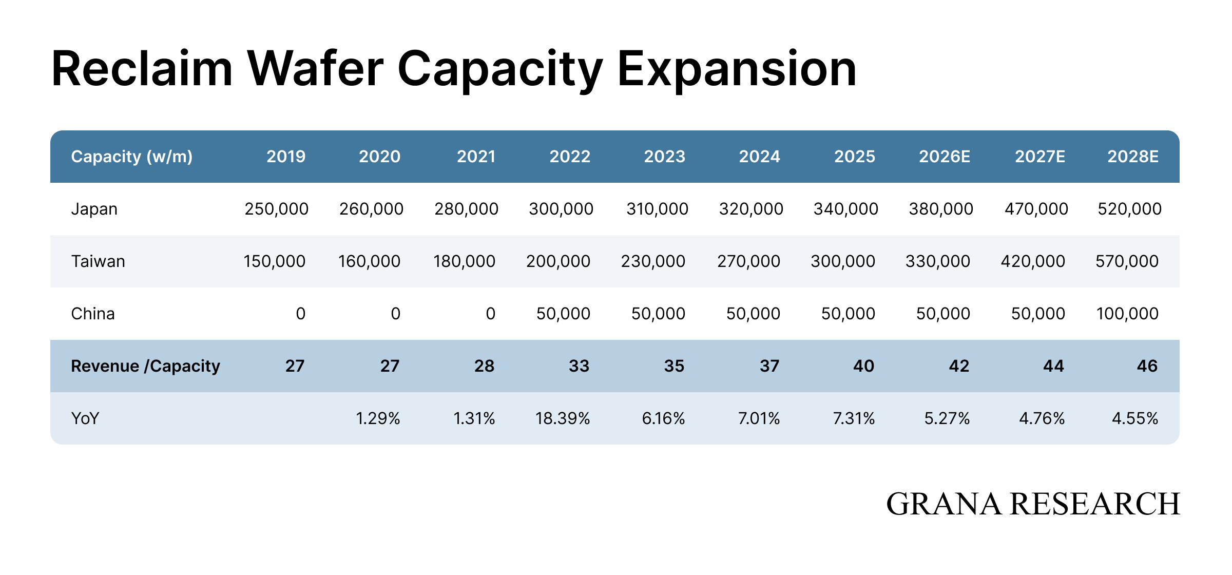
As discussed earlier, wafer reclaim is RS Technologies’ core business. Over the past five years, segment revenue has grown at a 19.2% compound annual growth rate, while operating margins have consistently remained in the high-thirties.
Segment revenue is driven by three key variables: a) available capacity, b) capacity utilization, and c) the average reclaim price per wafer. Ultimately, all three factors are determined by underlying demand, which we expect to accelerate over the coming years.
Despite serving a relatively limited number of customers, RS Technologies has increased revenue per unit of capacity by an average of 7.9% annually over the past five years. We expect this metric to grow at an average annual rate of 4.9% between 2026 and 2028, with the anticipated moderation reflecting the record pace of capacity additions.
We also expect the company’s capacity utilization to remain exceptionally high, supported by continued expansion of semiconductor manufacturing capacity and robust demand for its services.
As a result, we expect wafer reclaim revenue growth to accelerate from the current mid-teens to the high-twenties over the next several years. Segment operating margins are likely to come under pressure due to a significant increase in D&A expense. Nevertheless, we forecast operating profit to increase by approximately 77% between 2025 and 2028.
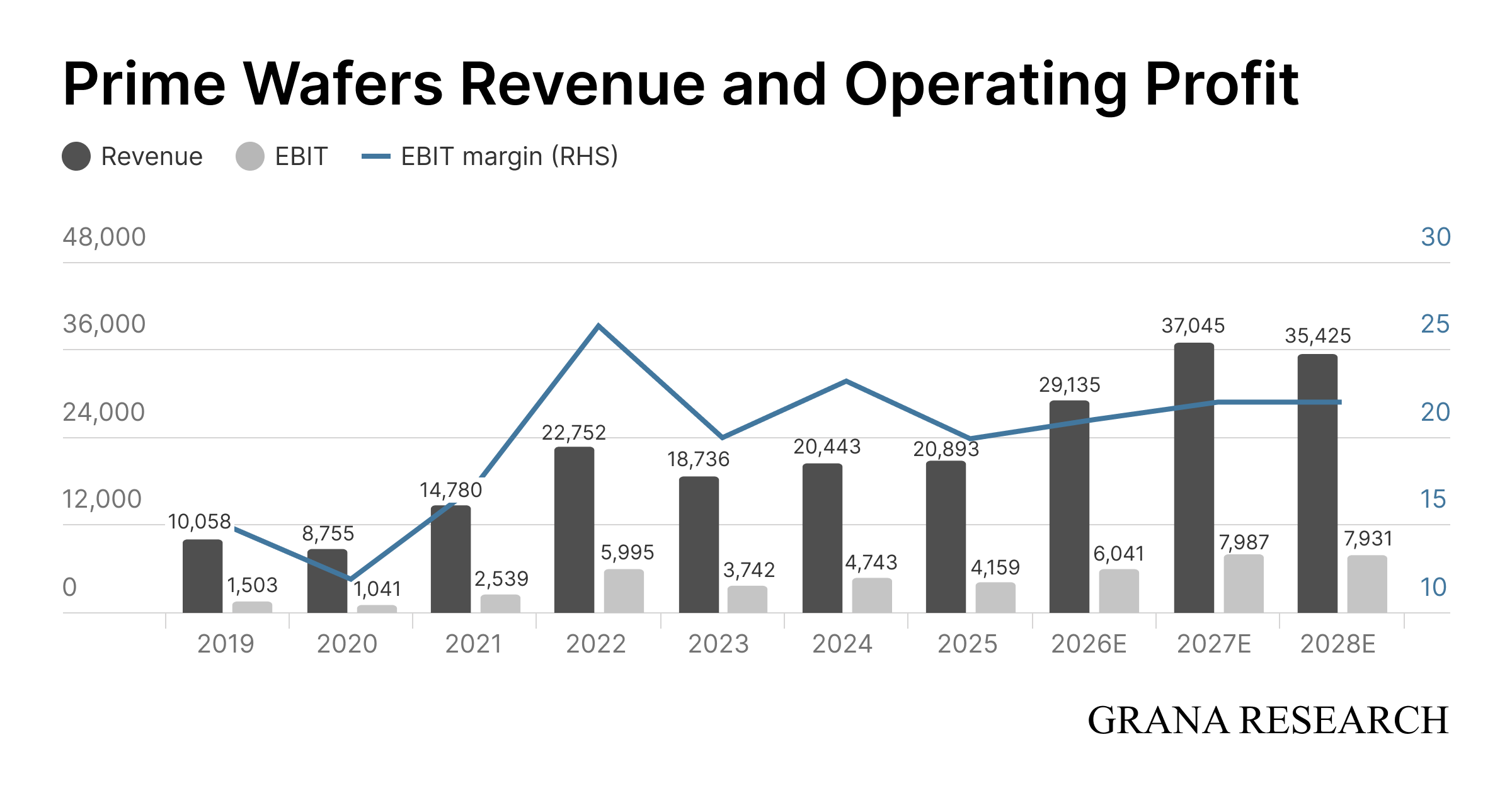
Until recently, the prime wafer business had been going through a deep downcycle. In 2024, despite a 36% increase in shipment volume, revenue grew by only 3.8%, as average selling prices declined by ~25%. In 2025, net sales totaled ¥20.8 billion, up 2.2% year over year, driven by a more than 20% year-over-year increase in 8-inch wafer shipment volume. On the other hand, the average unit price declined by ~10% year over year.
Notably, 2025 already showed the first signs of market stabilization. Average selling prices for power semiconductor wafers — the company’s core product — declined only modestly. The largest price declines were seen in general-purpose products, such as IGBT and memory wafers, which account for 20-30% of the company’s product mix.
In Q1 2026, prime wafer segment revenue increased by 32% year over year, while operating profit grew by 22% year over year, supported by ASP stabilization and higher shipment volumes. We believe RST is at the beginning of an upcycle in this segment. ASP for 8-inch wafers is expected to increase by 10-15% by the end of 2026. This is driven by extremely high capacity utilization at Chinese fabs (above 110% at industry leader Hua Hong) and rising prices for power semiconductors, such as IGBTs.
In addition, the share of production capacity dedicated to the structurally declining 5-inch and 6-inch wafer segments is expected to decrease from 41% to 32.5% by year-end, as RST plans to expand 8-inch capacity by 20% and 12-inch capacity by 50% year over year. Even assuming only a 10% increase in ASP by year-end, segment revenue growth could exceed 35%. It is worth noting that the sell-side consensus currently forecasts 26% year-over-year revenue growth for 2026.
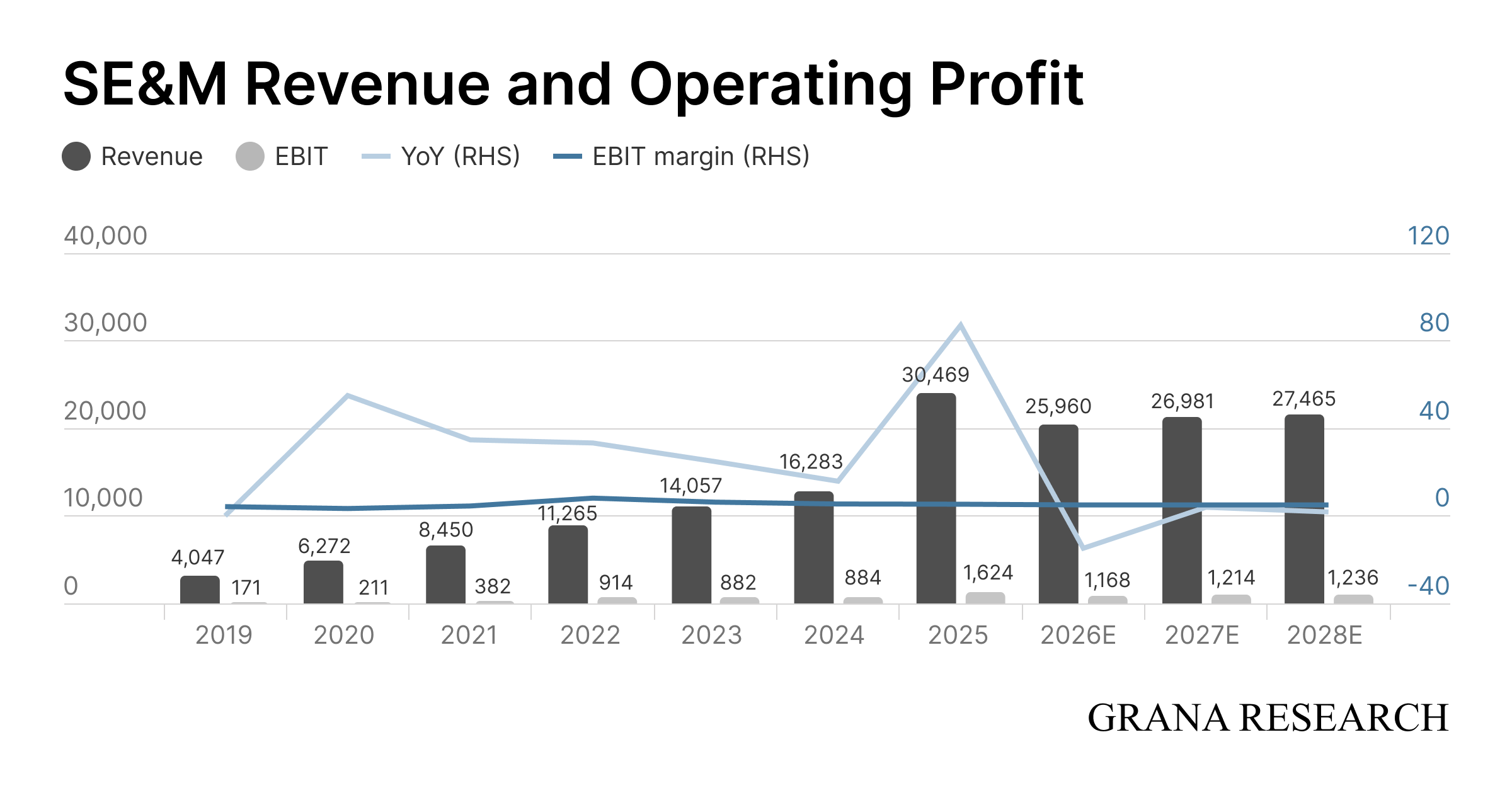
The Semiconductor Equipment and Materials business is likely to lag. Last year, approximately half of segment revenue came from RSPDH, the business acquired from Sony, generating ¥15 billion in revenue versus management’s original guidance of ¥10 billion. The outperformance was driven by earlier-than-expected deliveries of optical pickup modules under customer orders inherited as part of the acquisition. However, those accelerated shipments in 2025 effectively pulled forward revenue from future periods. As a result, we expect RSPDH revenue to decline in 2026. RST management is guiding for RSPDH revenue of ¥10 billion for the full year [15].
Weakness at RSPDH is likely to be partially offset by growth at DG Technologies and Union Electronics, as both businesses appear to be at the beginning of an upcycle. Nevertheless, we model a 13.7% year-over-year decline in segment revenue, assuming ¥4.5 billion of revenue at DGT and 3% growth across the remaining subsegments. We also forecast an operating margin of 5.3%, in line with the segment’s six-year historical average.
According to our model, we expect the company’s total revenue to grow at a compound annual growth rate of 15.3% between 2025 and 2028, while gross profit is projected to grow at a CAGR of 14.8%. Despite a significant increase in depreciation expense, we expect gross margin to remain broadly stable throughout the forecast period, driven by the increasing contribution of the higher-margin wafer reclaim business, whose share of total company revenue is expected to increase from 35.9% to 46.5%.
Benefiting from operating leverage, we forecast operating profit to grow at a CAGR of 19.5%, while net income is expected to increase at a CAGR of 19.8%. Our model does not assume any additional acquisitions, despite the company’s relatively aggressive approach to M&A.
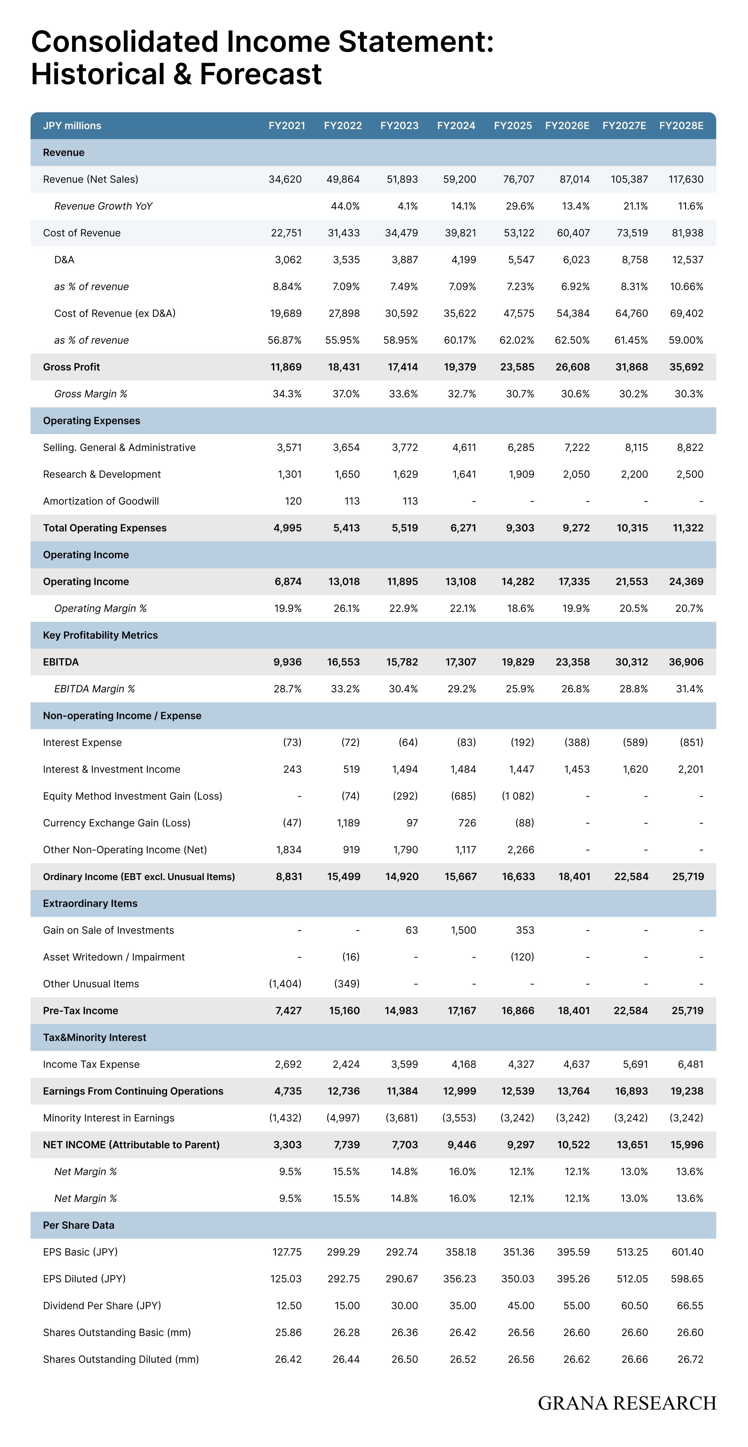
RS Technologies has presented its financial targets through 2028. According to our estimates, the company’s net income could exceed management’s guidance by ~5%, ~19%, and ~23% in 2026, 2027, and 2028, respectively. It is worth noting that management’s previous medium-term guidance, covering the periods through 2023 and 2026, also proved to be conservative [16] [17].
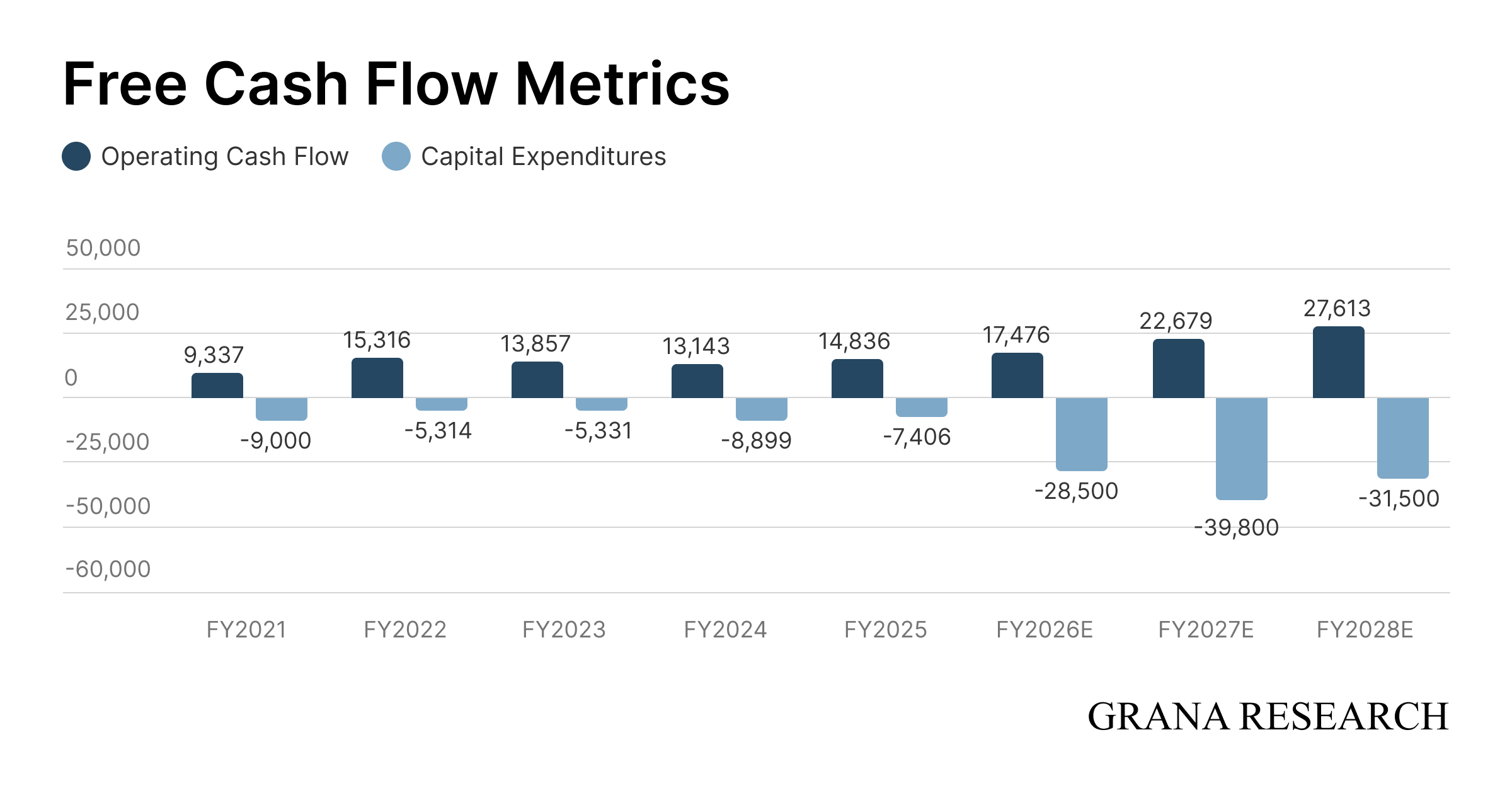
Despite continued growth in operating cash flow, we expect the company’s free cash flow to remain negative over the next several years. Nevertheless, RST’s net debt is likely to remain negative even if the planned investments are financed entirely through debt.
Valuation is the most important part of the investment case for the company. As discussed earlier, RS Technologies owns a 39.1% stake in GRITEK (688432 CH), a publicly listed Chinese manufacturer of silicon wafers. As of July 27, GRITEK’s market capitalization stood at RMB 49.86 billion (~$7.36 billion). Accordingly, RS Technologies’ 39.1% stake is worth ~$2.9 billion, while RST itself has a market capitalization of only $926.7 million. In other words, the market is assigning a negative value to the company’s profitable and rapidly growing wafer reclaim business.
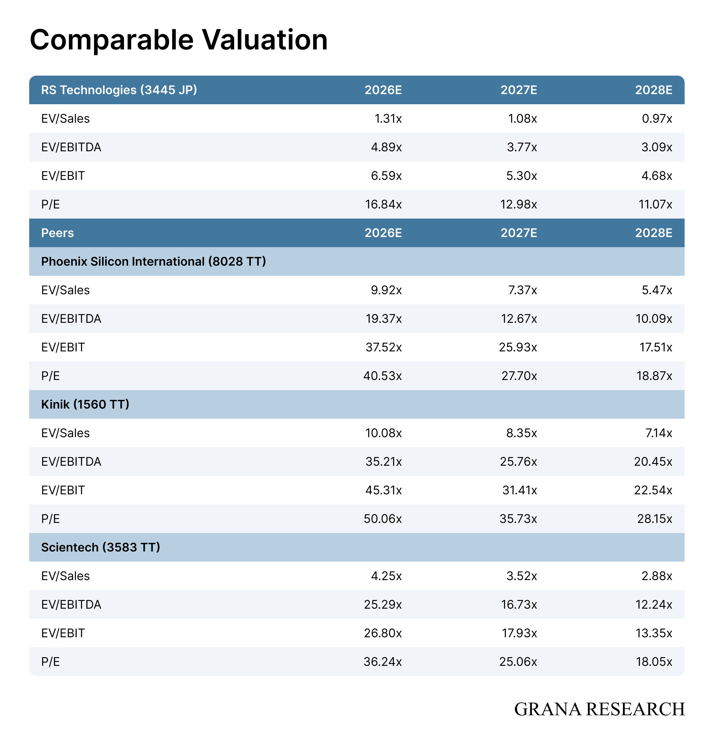
The gap is equally pronounced from the perspective of a traditional comparable valuation. The wafer reclaim market is highly concentrated, with RS Technologies’ largest competitors being the Taiwanese companies Phoenix Silicon International (8028 TT), Kinik (1560 TT), and Scientech (3583 TT). The figure below compares RST’s forward valuation multiples (based on our estimates) with those of its peers (based on sell-side consensus). RS Technologies is trading at a substantial discount to its peers across valuation metrics.
It is worth noting that management is well aware of the company’s significant undervaluation — and says so explicitly. Investor Relations acknowledges that RST’s valuation multiples are materially below those of comparable companies and that senior management fully recognizes this. Moreover, the company’s CEO closely monitors the share price on a daily basis and, as a major shareholder, is personally dissatisfied with the company’s current valuation.
There are also multiple avenues to unlock shareholder value. In our view, the most straightforward approach would be to deconsolidate the prime wafer business by selling shares in GRITEK, followed by share repurchases or the payment of special dividends. Another effective option would be a spin-off of the wafer reclaim business. As a standalone company, this business could potentially be worth several times more than the current market value of RS Technologies as a whole.
Key Risks / Bear Case
Loss of Share at TSMC
RS Technologies is the global leader in the wafer reclaim market, with an estimated market share of roughly one-third. The issue is that this represents the market of yesterday. In the fastest-growing part of the industry — advanced process nodes at the world’s largest customer — TSMC — the company has been losing ground for several years to Taiwan’s Phoenix Silicon International (PSI).
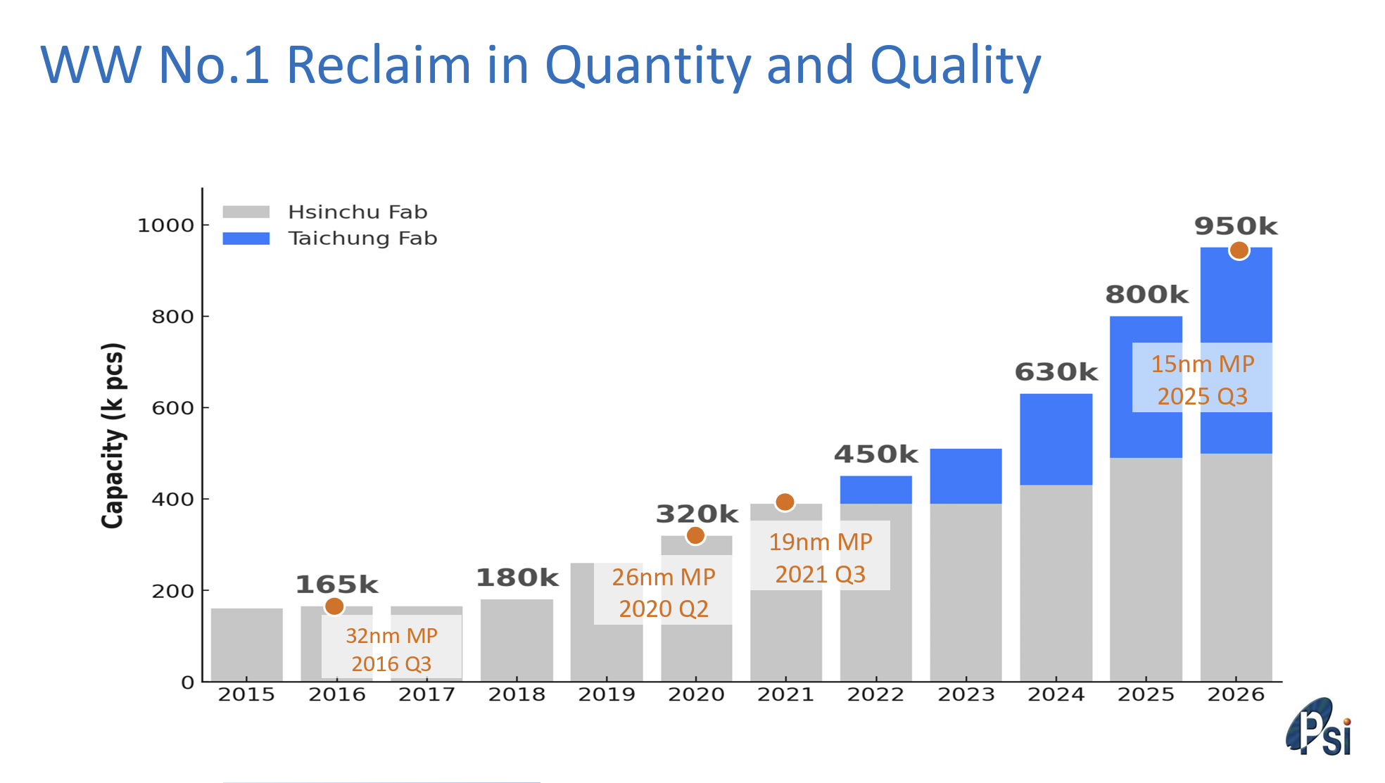
RS Technologies denies that it has lost market share. However, the publicly available data suggests otherwise. Although PSI has historically been smaller than RST, it plans to increase its 12-inch wafer reclaim capacity from 630,000 wafers per month in 2024 to 950,000 wafers per month by 2026.
After conducting a series of expert interviews, we concluded that TSMC has increasingly favored the local Taiwanese supplier, particularly at advanced process nodes, for three reasons. First, quality control. Shipping wafers back to Taiwan by air after processing in Japan introduces edge defects and surface particle contamination, which is unacceptable for leading-edge manufacturing processes.
Second, logistics costs. Unlike prime wafers, which are worth approximately $80-100 per wafer and for which transportation costs are relatively insignificant, wafer reclaim is a much lower-value service, making logistics a meaningful component of the total cost.
Third — and most importantly — working capital. RS Technologies’ end-to-end door-to-door turnaround time is approximately three to four weeks, whereas PSI, located just three minutes from TSMC’s fabs, completes the cycle in about one week. Given TSMC’s scale, the additional three weeks of wafers tied up in the supply chain represent a significant amount of working capital.
One industry expert described the situation as follows:
Interviewer
When you talk about TSMC, obviously PSI are known to be doing the wafer reclaim business with TSMC particularly focused on their more advanced nodes, for example two nm. TSMC by all accounts used to use more a Japanese competitor and Phoenix has taken market share. My understanding is that they took market share because their Japanese competitor essentially just didn’t have enough capacity. What do you know about the situation with regard to TSMC, the reason for Phoenix’s market share gain and how they compare versus in the industry to the Japanese competitor?
Consultant in Semiconductor Wafer
Yes, RS Technologies. The couple reasons, number one is in the earlier stage like 15 years ago, RS Technologies are doing much better than PSI because PSI, if you have been inside their facility, they have a lot of problems. For example, many steps are manual and not as automatic as the RS Technologies. Also, their quality control and the EAR are not as good as RS Technologies as well.
However, there are a couple points. Number one is, recycle recurring wafer. TSMC always prefer the local manufacturing or local supply due to couple reasons. Number one is the quality control because when the ship to Japan and ship-back which means the quality control sometimes the shift can happen especially when logistics like an aircraft.
You take the passenger aircraft. Your life is sometimes got thrown in the crack. Similar situation happens during the wafer reclaimed specially ship-back. You ship to Japan, that’s fine. When you finish everything and ship-back, when the transportation is now well taken care then the forearm particle or the wafer edge chipping or crack can happen which means the quality control is always a problem.
This is why TSMC won the local supply and as close as possible. That’s the reason if you know that PSI headquarter to TSMC it’s just around by scooter maybe three minutes, two to three minutes, this is at most. In Taichung and in Thailand, PSI have the facility as well. As you can imagine in the past, TSMC can ship all the wafer from Taiwan to Japan.
How come they cannot just have one facility in Taiwan and ship all the wafer around Taiwan to that point? This is the proof that TSMC want PSI attached to their facility and do the local supply and shorten the supply chain because the 1) quality and 1) is the price. Since we can cut the transportation price, then it can reflect to the cost of the reclaim wafer.
The transportation you can almost ignore. However, for the reclaim wafer, it’s not high price. Unfortunately you have to try to set the cost as much as possible. The transportation cost is another thing as well. 3) is maybe the most important because when you do the wafer reclaim, which means the supply chain, there’s a lot of wafer accumulated in the whole supply chain.
The TSMC should wafer until the wafer go back to TSMC. In RS Technologies from door-to-door means day one leave the TSMC door until the day that arrive TSMC door again, it takes around like three to four weeks. I think you get a similar number as well. It means on average sent to RS Technologies, you accumulate four weeks wafer volume in the supply chain. It means money. However, if you use PSI, it takes around just one week.
Four weeks versus one week, the money accumulated right there is a significant, especially when TSMC is big enough. That is also the reason why the Micron Technology in Taichung, they use Kinik, the competitor of PSI as they work on Korean partner as well just because of the same reason. The money accumulated in the supply chain sent to RS Technologies four weeks. You can imagine the amount TSMC uses every single day. Four weeks versus one week is a significant difference. Quality and the shipping cost and all the total amount of money accumulated right there.
As early as January 2025, PSI, while explaining its capacity expansion plans, explicitly cited the overseas expansion of one of its key customers — rapidly increasing production of leading-edge chips in the United States — as one of the main growth drivers. The company did not identify the customer by name, but at the time there was only one manufacturer producing 4nm leading-edge chips in Arizona.
We would also highlight the company’s response. We were told that PSI’s expansion plans were difficult for them to understand, that the competitor was not yet fully utilizing its existing capacity, and that TSMC would not, in any case, rely on a single supplier.
In our view, it is unlikely that one of the largest players in this highly concentrated market — one that has consistently gained market share in recent years — would undertake a major capacity expansion without coordination with TSMC, particularly given that RST itself invests only after securing customer commitments. The argument that TSMC will not rely on a single supplier is, strictly speaking, correct. However, it does not suggest that RST is in a position to increase its market share.
Capital Allocation
Capital allocation — one of the most important considerations for any disciplined investor — is one of the weaker aspects of the RS Technologies investment case.
The wafer reclaim business accounts for only one-sixth of the group’s assets while generating approximately two-thirds of operating profit. By contrast, the prime wafer business in China absorbs roughly two-thirds of the group’s assets yet contributes only about one-quarter of operating profit. Moreover, that profit includes Chinese government subsidies. Excluding these subsidies, the core wafer reclaim business would account for approximately 71-75% of the group’s operating profit.
During our discussion with the company, management explicitly acknowledged the difference in profitability between the two businesses. Return on invested capital (ROIC) exceeds 20% in the wafer reclaim business but is below 5% in the prime wafer business. At the same time, demand for reclaimed wafers is so strong that RS Technologies is forced to turn away some customers due to insufficient capacity. Nevertheless, management continues to allocate a significant portion of capital to substantially lower-return businesses.
A notable example is the energy project, to which the company committed ~¥8 billion (~$49 million) earlier this year. Commercial operation is not expected to begin until October 2029. Formally, the investment is justified by its vertical linkage to subsidiary LE System, which manufactures electrolytes for vanadium redox flow batteries. In practice, however, RS Technologies is entering a capital-intensive infrastructure business where the group currently lacks any obvious operational expertise, competitive advantage, or pricing power [18].
This capital allocation policy has resulted in a sustained decline in the group’s return on invested capital. While the trend may begin to reverse over the coming years as the wafer reclaim business accounts for a larger share of earnings, the underlying issue remains unchanged: capital allocation discipline continues to be one of RS Technologies’ key weaknesses. In our view, if management concentrated its resources on the company’s core business, the market would assign a materially higher valuation to RS Technologies.
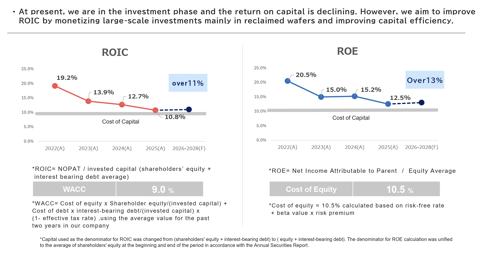
The explanation we received, in our view, accurately reflects management’s underlying rationale. Because the wafer reclaim market is relatively small, the company is constantly searching for a “second cash cow.” This explains its acquisitions, expansion into prime wafer manufacturing in China, and investments in the energy sector. We believe this approach is misguided for three reasons.
First, it is difficult to argue that market size represents a genuine constraint when the company already controls roughly one-third of the market and is still unable to satisfy existing demand. The real constraint is production capacity, which can be addressed through additional investment in a business generating returns on invested capital above 20%.
Second, the wafer reclaim market is growing faster than one might expect based solely on semiconductor production volumes. The transition to more advanced process nodes dramatically increases the number of test wafers required for each finished wafer. As a result, this is not a mature market with limited growth potential, but rather a niche benefiting from a structural acceleration in demand.
Third — and most importantly — the objective of a public company is not to maximize its own size, but to maximize shareholder value. If high-return investment opportunities within the core business are genuinely exhausted, excess capital should be returned to shareholders, who can allocate it more efficiently themselves. Diversifying into businesses generating 3-5% returns does not solve the problem of a “small market” — it merely reduces the group’s overall return on invested capital.
Conclusion
RS Technologies has evolved from a distressed asset into one of the leaders in a small, capital-intensive, yet structurally growing oligopolistic market. The core of the investment case — the wafer reclaim segment — is a high-quality business operating at 100% capacity utilization, with long-term demand supported by two structural drivers: the global expansion of semiconductor fabrication capacity and the migration to advanced process nodes, which increases reclaimed wafer consumption by 3-4x for the same level of fab capacity.
The investment case is not without flaws, and we do not seek to downplay them. The most significant is the gradual loss of share at TSMC in the fastest-growing leading-edge process nodes, where Phoenix Silicon has been gaining ground. RST’s decision not to build a wafer reclaim facility in Arizona appears disciplined from a margin perspective, but in practice it meant declining the opportunity to participate in the fastest-growing part of the supply chain of its largest customer — an opportunity that Phoenix Silicon accepted. The second weakness is capital allocation. Despite operating a core business constrained only by capacity and generating ROIC above 20%, management continues, in its search for a “second cash cow,” to allocate capital to businesses earning 3-5% returns — including the Chinese prime wafer business and an infrastructure project related to vanadium redox flow batteries (VRFBs) — thereby diluting the group’s overall return on capital.
Even after fully accounting for these negative factors, however, RS Technologies’ valuation appears unjustifiably low — both from the perspective of comparable company valuation and from the standpoint of simple economic logic.
On a relative valuation basis, the company trades at a substantial discount to its closest peers despite a core business of comparable or superior quality and growth. From a fundamental perspective, the disconnect is even more striking: RST’s 39.1% stake in publicly listed GRITEK alone is worth approximately $2.9 billion, while RS Technologies’ entire market capitalization is only around $926.7 million. In other words, the market is assigning a negative value to a profitable, rapidly growing wafer reclaim business generating ROIC above 20% and operating at full capacity utilization.
Such a valuation dislocation is unlikely to persist indefinitely. Management — and particularly CEO and controlling shareholder Ho Nagayoshi — recognizes the company’s undervaluation and has several obvious levers to unlock shareholder value. Logical steps could include deconsolidating the prime wafer business through the sale of GRITEK shares, followed by share repurchases or special dividends, or alternatively a spin-off of the wafer reclaim business, which, as a standalone public company, could plausibly be worth several times the current market capitalization of RS Technologies. Even under a conservative scenario in which market share losses at TSMC continue, and capital allocation remains suboptimal, the valuation discount is simply too large to justify. At today’s share price, investors are effectively acquiring the company’s high-growth core business for free, while any future value-unlocking initiatives represent embedded upside optionality.
Sources
[1] https://www.rasa.co.jp/company/history/history.html
[2] https://yunogami.net/ej/_src/1020/EJ11年3月号.pdf
[3] https://www.rs-tec.jp/en/press/press_images/20180410.pdf
[4] https://shachomeikan.jp/presidents/detail/10062694/5195
[5] https://bridge-group.co.jp/ipo_media/6978/
[6] https://toyokeizai.net/articles/-/935426?page=3
[7] https://www.rs-tec.jp/corporate/history/
[8] https://contents.xj-storage.jp/xcontents/AS02916/68cc9041/1a69/4951/8014/b845895bed3a/140120260514534869.pdf
[9] https://www.sumcosi.com/english/ir/library/presentations/
[10] YouTube
[11] https://contents.xj-storage.jp/xcontents/AS02916/4dfb2d10/d8e7/4345/b803/f1e0c7b10577/140120260410502015.pdf
[12]https://www.siltronic.com/fileadmin/investorrelations/2025/Q4/20260312_Siltronic_InvestorPresentation.pdf
[13] https://investor.ti.com/static-files/fc9d9346-cf77-40db-902a-e9961e9c5736
[14] https://www.listcorp.com/asx/cmg/critical-minerals-group-limited/news/investor-presentation-3364878.html
[15] https://contents.xj-storage.jp/xcontents/AS02916/ca064325/4738/4e9c/9256/af5d7cf9ca3d/140120260514534875.pdf
[16] https://contents.xj-storage.jp/xcontents/AS02916/30bd651d/ce27/42a5/a881/1d796c683425/20230214172151528s.pdf
[17] https://contents.xj-storage.jp/xcontents/AS02916/f053a8d2/a8d9/4b7b/92e3/bee3912a8d8b/140120240216538951.pdf
[18] https://prtimes.jp/main/html/rd/p/000000007.000110789.html?utm_source=chatgpt.com
[19] https://www.psi.com.tw/en/share_news2.asp
[20] AlphaSense
[21] Bloomberg
Disclaimer / Disclosures
The information contained in this report is provided solely for informational and educational purposes and does not constitute investment advice, investment research under applicable securities regulations, an offer to sell, or a solicitation to buy any security or financial instrument.
The opinions expressed in this report reflect the author’s views as of the date of publication and are subject to change without notice. This report has been prepared without regard to the specific investment objectives, financial situation, or particular needs of any individual investor. Readers should conduct their own independent research and seek professional financial, legal, tax, or other advice before making any investment decision.
The analysis presented in this report is based on information believed to be reliable, including publicly available sources, company disclosures, industry publications, and discussions with market participants. While reasonable efforts have been made to ensure the accuracy of the information, no representation or warranty, express or implied, is made as to its accuracy, completeness, or reliability. Any estimates, assumptions, or forecasts represent the author’s judgment and are inherently subject to uncertainty.
This report contains forward-looking statements, including expectations regarding future financial performance, industry trends, market developments, and company prospects. Such statements involve known and unknown risks, uncertainties, and assumptions that may cause actual results to differ materially from those expressed or implied. No assurance can be given that any projections or forecasts will be realized.
The author may hold, establish, increase, reduce, or dispose of positions in any securities discussed in this report at any time without prior notice. Such positions may create potential conflicts of interest. Nothing in this report should be interpreted as a recommendation to buy, sell, or hold any security.
To the fullest extent permitted by applicable law, the author disclaims any liability for any direct or indirect loss arising from the use of, or reliance upon, the information contained in this report.
$UMC $STM $PLAB
any comments?
Grana, not many people are doing research pieces as in depth as you are, even few are dropping 10,000+ word pieces that are 100% human.
A large part of the bull case is their holding in GRITEK, curious if you know how hard it is to liquidate that holding. Of course as you mentioned they sold part of their holding but will it be possible to liquidate the entire holding without seriously depressing GRITEK's stock?
Excited to hear your thoughts.
I Really appreciate the quality of your work and looking forward to reading more deep dives!